Substrate heating apparatus and semiconductor fabrication method

Active Publication Date: 2008-09-04
CANON ANELVA CORP
View PDF9 Cites 16 Cited by
  • Summary
  • Abstract
  • Description
  • Claims
  • Application Information

AI Technical Summary

Benefits of technology

[0024]It is, therefore, an object of the present invention to provide a substrate heating apparatus and semiconductor fabrication method capable of performing a uniform substra

Problems solved by technology

However, SiC crystals sometimes break when implanting impurity ions accelerated by high energy.
That is, when forming a MOSFET or the like by using an SiC substrate having a roughened surface, a gate insulating film and the like are formed on the roughened surface of the SiC substrate, so

Method used


Image

  • Substrate heating apparatus and semiconductor fabrication method
  • Substrate heating apparatus and semiconductor fabrication method
  • Substrate heating apparatus and semiconductor fabrication method

Examples


Example

First Embodiment

[0043]FIGS. 3A and 3B are views for explaining a preferred embodiment of the present invention.

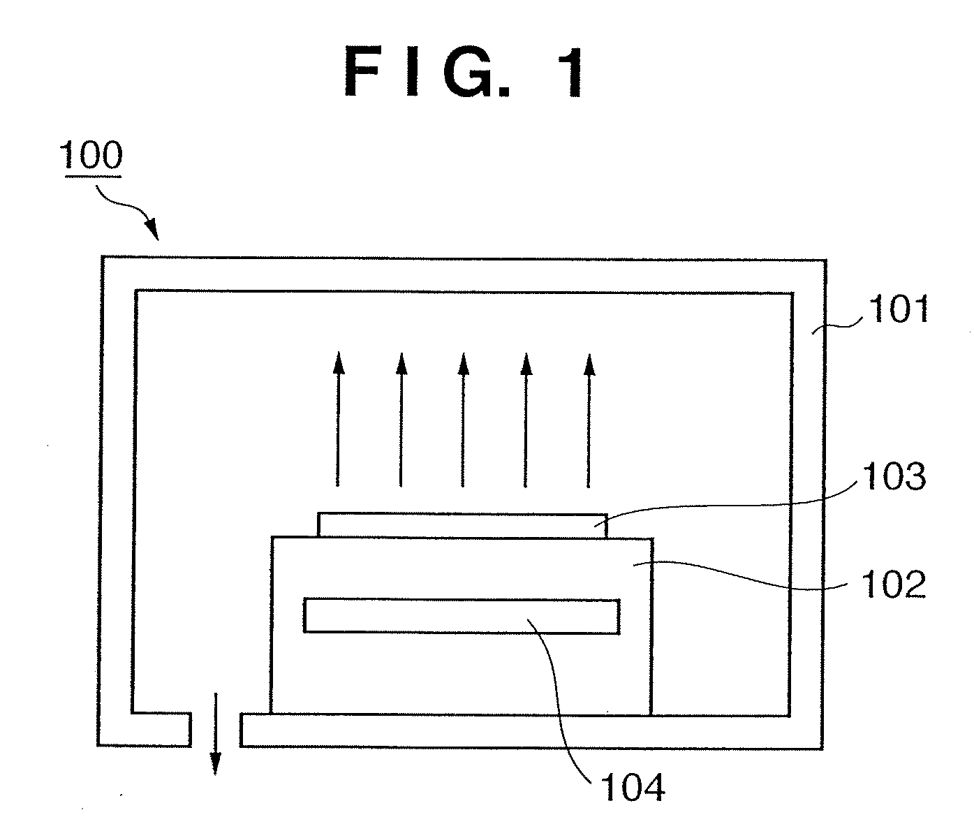
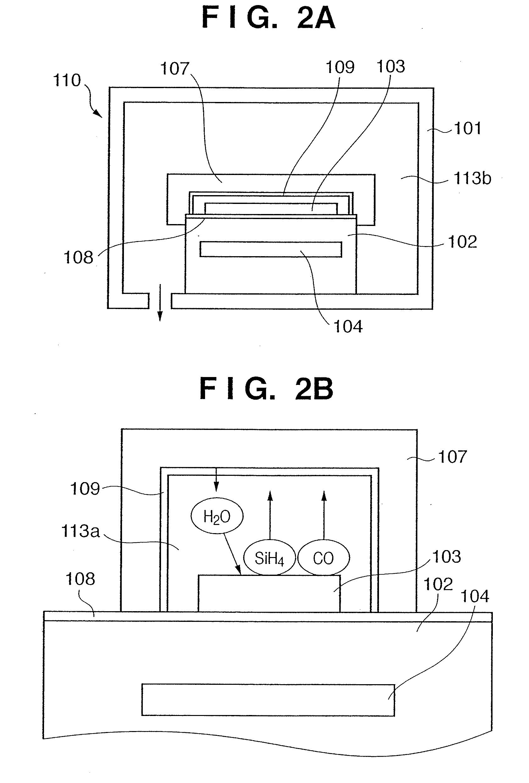
[0044]A substrate heating apparatus 10 shown in FIG. 3A includes a heating means 4 for heating a substrate (semiconductor substrate) 3 placed in a process chamber 1 that can be evacuated by an evacuating means (not shown), and heats the substrate 3 placed in the process chamber 1 by the heating means 4.

[0045]The heating means 4 is incorporated into a suscepter 2, and the substrate 3 to be heated is placed on the upper surface of a substrate support in the upper portion of the suscepter 2.

[0046]In this manner, the suscepter 2 is installed between the heating means 4 and substrate 3.

[0047]Also, a heat receiving member for receiving the heat from the heating means 4 via the suscepter 2 is installed to oppose the suscepter 2 with the substrate 3 being sandwiched between them.

[0048]In the embodiment shown in FIGS. 3A and 3B, this heat receiving member includes a top plate 7a, an...

Example

Second Embodiment

[0104]FIGS. 5A to 5C are views for explaining the second embodiment of the present invention.

[0105]In the second embodiment shown in FIGS. 5A to 5C, a heat receiving member is a cover member 22 placed on an upper end opening 23 of a cylindrical support member 21 to close the upper end opening 23.

[0106]That is, in this embodiment shown in FIGS. 5A to 5C, the cap 17 explained in the embodiment shown in FIGS. 3 and 4 comprises the cylindrical support member 21, and the cover member 22 placed on the upper end opening 23 of the cylindrical support member 21 to close the upper end opening 23.

[0107]A step portion 26 formed on the inner circumferential wall of a middle portion between the upper end opening 23 and a lower end opening 30 of the cylindrical support member 21 supports the edge of the bottom surface of a substrate 3 to be heated.

[0108]The cylindrical support member 21 in which the edge of the bottom surface of the substrate 3 to be heated is supported by the ste...

Example

Third Embodiment

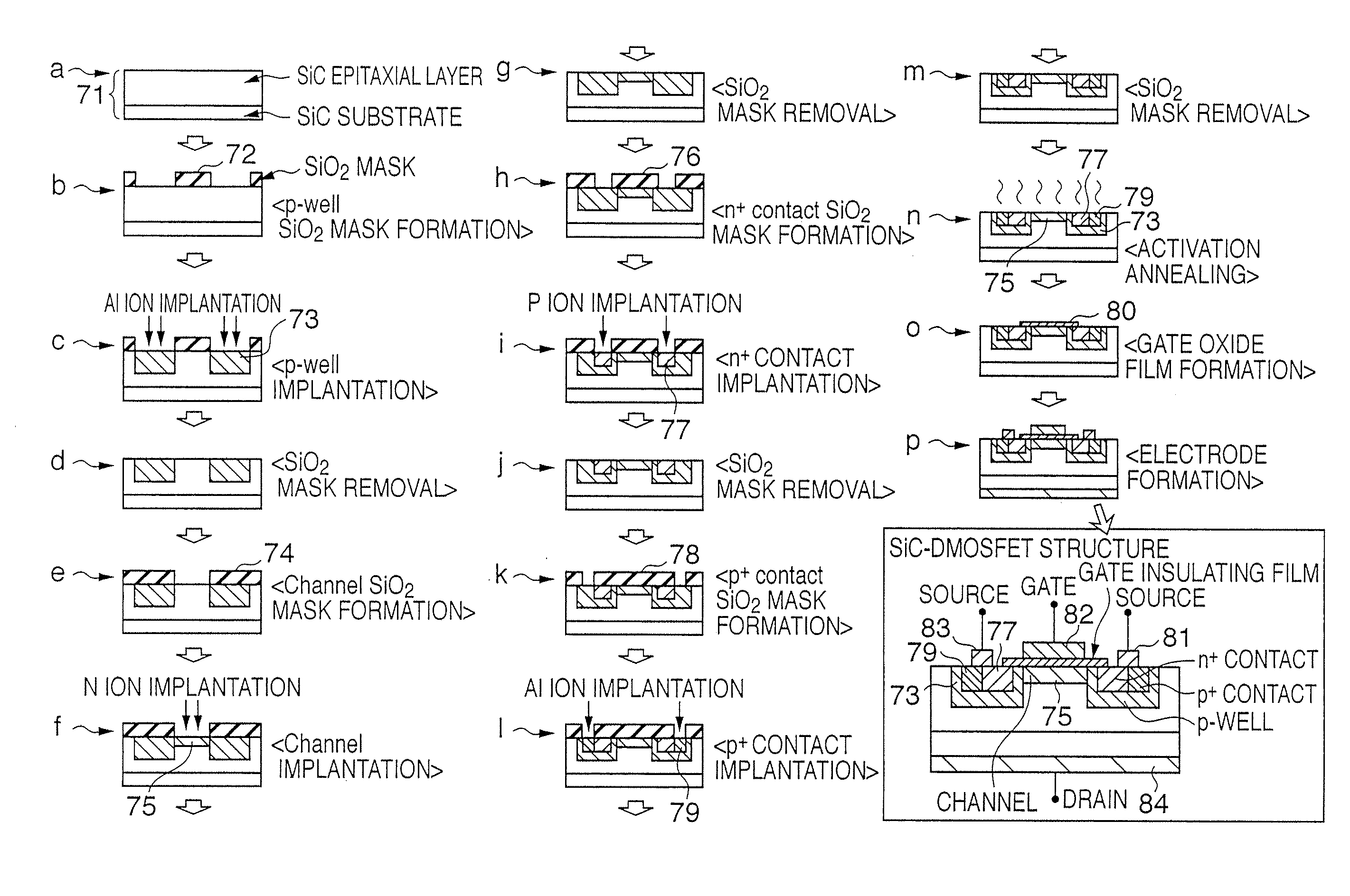
[0123]A method of annealing a well region 62 formed by implanting an impurity into a silicon carbide (SiC) substrate 61 will be explained below with reference to FIGS. 6A and 6B.

[0124]After sacrificial oxidation and hydrofluoric acid processing are performed, an SiO2 film and the like are formed on the silicon carbide (SiC) substrate 61, a mask 63 is formed by lithography and dry etching, and aluminum ions as an impurity are implanted by an ion implantation apparatus or the like (not shown) in order to selectively form the well region 62 in the silicon carbide (SiC) substrate 61 (FIG. 6A).

[0125]Note that in this embodiment, TMA (TetraMethyl Aluminum) as an impurity source is excited by a plasma, and Al ions to be implanted are extracted by an extractor electrode and analyzer tube and implanted. However, it is also possible to excite aluminum as a source by a plasma, extract aluminum ions to be implanted by an extractor electrode and analyzer tube, and ion-implant the...


PUM


Abstract

A substrate heating apparatus having a heating unit for heating a substrate placed in a process chamber which can be evacuated includes a suscepter which is installed between the heating unit and a substrate, and on which the substrate is mounted, and a heat receiving member which is installed to oppose the suscepter with the substrate being sandwiched between them, and receives heat from the heating unit via the suscepter. A ventilating portion which allows a space formed between the heat receiving member and substrate to communicate with a space in the process chamber is formed.

Description

BACKGROUND OF THE INVENTION[0001]1. Field of the Invention[0002]The present invention relates to a substrate heating apparatus and semiconductor fabrication method used in a semiconductor substrate heating process.[0003]2. Description of the Related Art[0004]Annealing for processing a semiconductor substrate at a high temperature has been conventionally extensively used. For example, a process of activating an ion-implanted impurity and a rapid thermal process (rapid thermal anneal) for, for example, recovering crystal defects caused by ion implantation are widely performed.[0005]When a silicon carbide (SiC) substrate is used, for example, the material characteristics suppress thermal diffusion, and local dopant control uses ion implantation. However, SiC crystals sometimes break when implanting impurity ions accelerated by high energy. A high-temperature heating process is performed to electrically activate the implanted impurity by recrystallizing the almost amorphousized sic.[000...

Claims


Application Information

Patent Timeline
IPC IPC(8): H01L21/425F26B19/00
CPCH01L21/046H01L21/67103H01L29/7802H01L29/0878H01L29/66068H01L21/67109H01L21/324
Inventor SHIBAGAKI, MASAMINUMAJIRI, KENJIEGAMI, AKIHIROKUMAGAI, AKIRAAKIYAMA, SUSUMU
Owner CANON ANELVA CORP
Why Eureka
Try Eureka