

Selective copper-silicon-nitride layer formation for an improved dielectric film/copper line interface
a technology of copper-silicon-nitride and dielectric film, which is applied in the direction of liquid surface applicators, pretreated surfaces, coatings, etc., can solve the problems of copper being undetectedly peeled during polishing, the tendency of silicon dioxide to diffuse into silicon dioxide, silicon and other adjacent dielectric materials, and the failure of integrated circuits, etc., to achieve the effect of improving the adherence to the underlying copper interconnect and reducing the dielectric constant (
- Summary
- Abstract
- Description
- Claims
- Application Information
AI Technical Summary
Benefits of technology
Problems solved by technology
Method used
Image

Examples
Embodiment Construction
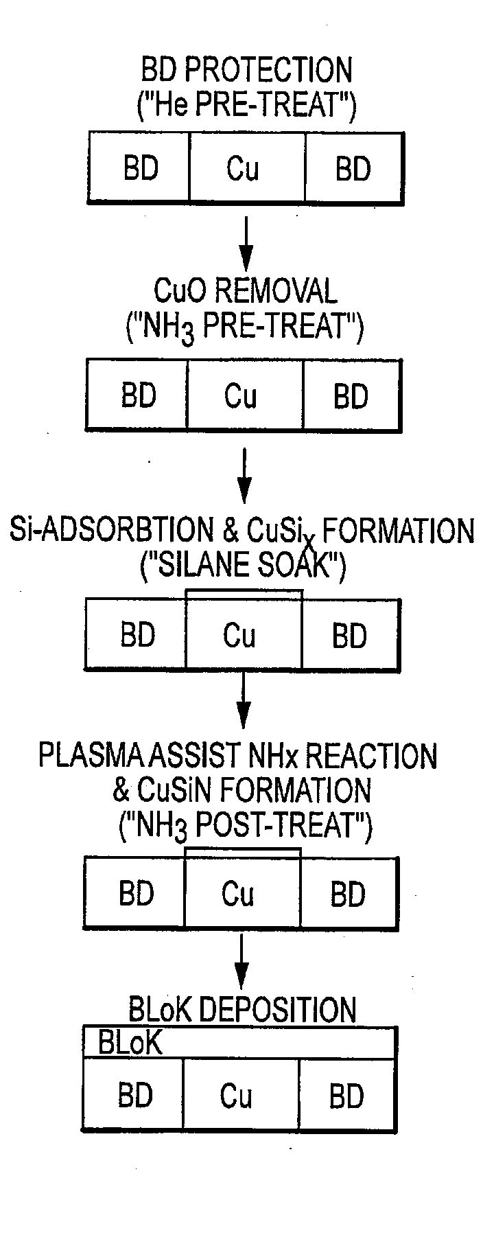
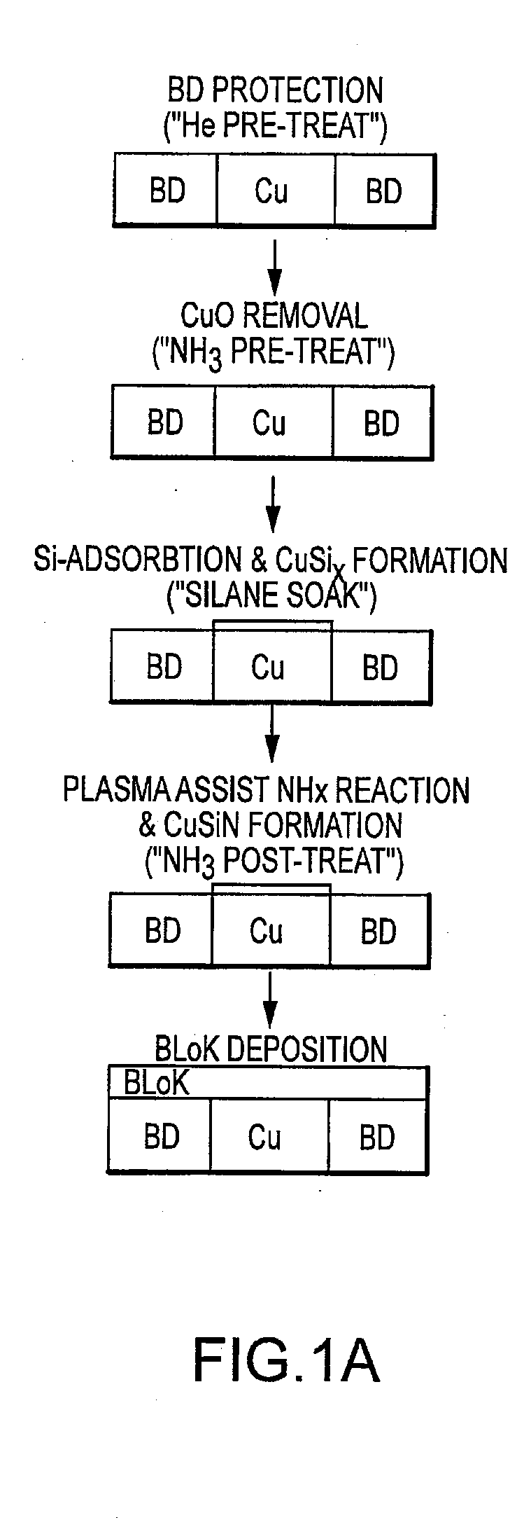
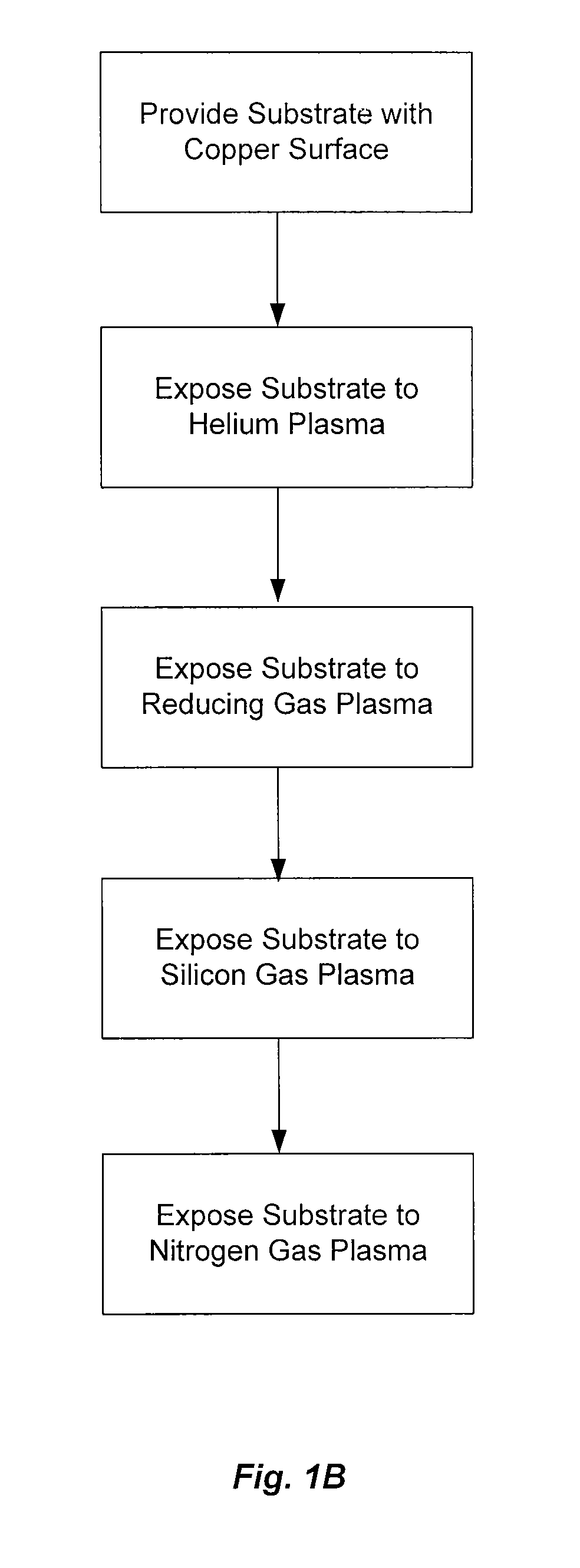
[0026]With the advent of copper dual damascene, dielectric copper barriers are becoming the cornerstone for back end of line device reliability. The interface between copper and dielectric barrier is often the fastest diffusion path for the EM of copper, and that the improved adhesion of barrier film to copper increases the lifetime of EM. The present invention includes processes for engineering an interface between copper and a barrier layer to improve the EM performance. These processes can improve EM performance up to an order of magnitude or more compared to conventional barrier layer deposition by forming a thin (˜100 Å or less) CuSixNy adhesion layer between the copper film and barrier layer.
[0027]The present processes for forming the CuSixNy barrier layer can achieve the following results: (1) a small change in the dielectric constant (κ) of the nearby dielectric material; (2) a small increase in the sheet resistance (Rs) of the copper film; (3) a long EM lifetime; and (4) a ...
PUM
| Property | Measurement | Unit |
|---|---|---|
| Temperature | aaaaa | aaaaa |
| Temperature | aaaaa | aaaaa |
| Electrical resistivity | aaaaa | aaaaa |
Abstract
Description
Claims
Application Information