[0012]An
advantage of some aspects of the invention is that it provides an organic transistor exhibiting a superior mobility, on / off ratio and
threshold voltage and low-dispersion characteristics, and a method for manufacturing the organic transistor. Another
advantage of the invention is that it provides an electronic apparatus including the organic transistor, exhibiting superior electrical characteristics.
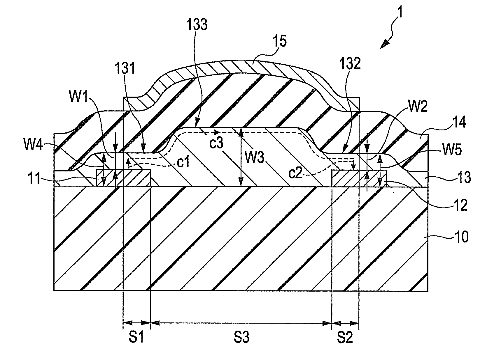
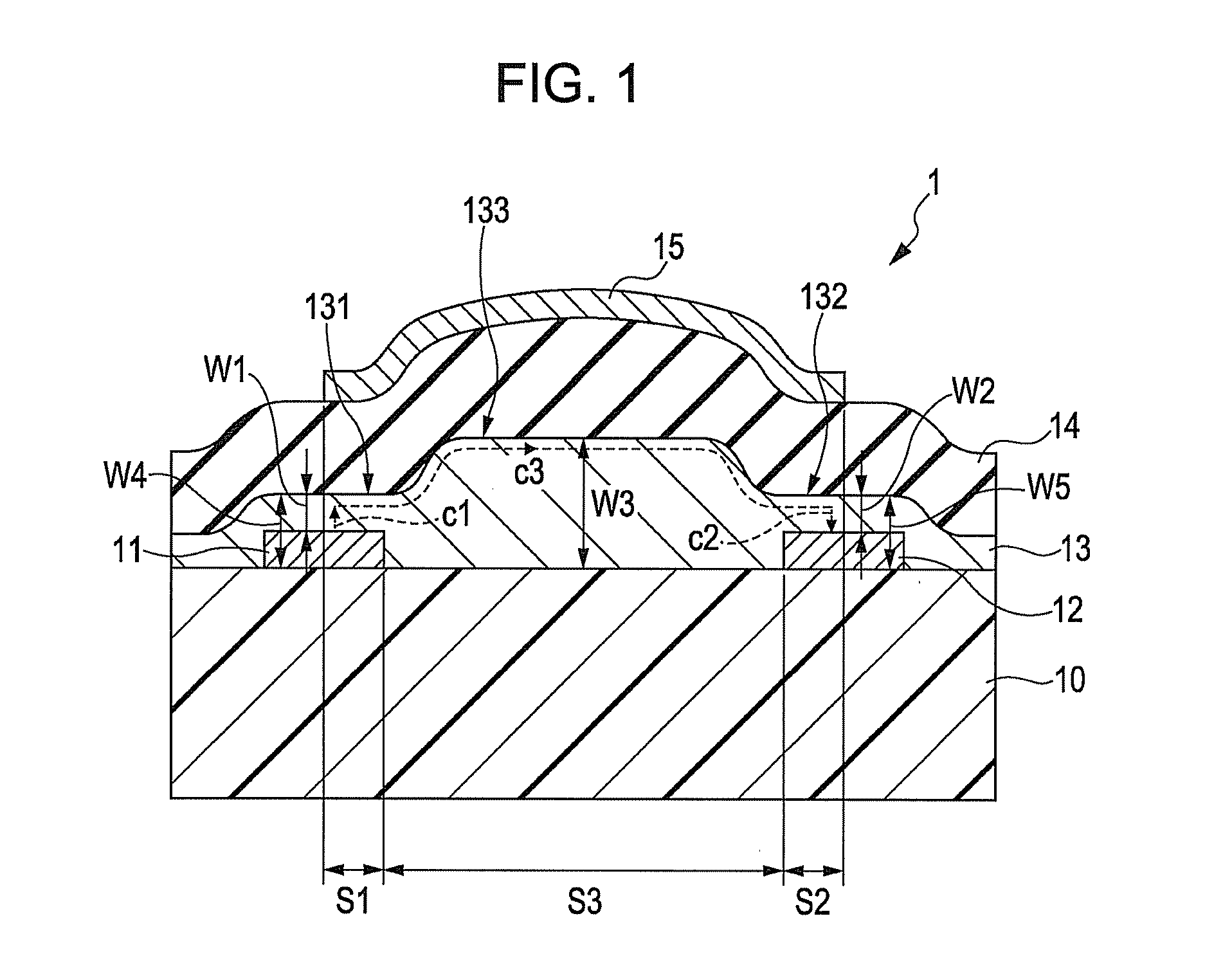
[0013]According to an aspect of the invention, an organic transistor is provided which includes a source electrode and a drain electrode, an organic semiconductor layer disposed across between the source electrode and the drain electrode, and a gate electrode opposing the source and drain electrodes with the organic semiconductor layer and an gate insulating layer therebetween. The organic semiconductor layer includes a first semiconductor portion in a region where the gate electrode and the source electrode oppose each other, a second semiconductor portion in a region where the gate electrode and the drain electrode oppose each other, and a third semiconductor portion between the first semiconductor portion and the second semiconductor portion. The first semiconductor portion, the second semiconductor portion, and the third semiconductor portion satisfy the relationships W1<W3 and W2<W3, wherein W1 represents the average thickness of the first semiconductor portion, W2 represents the average thickness of the second semiconductor portion, and W3 represents the average thickness of the third semiconductor portion. In this structure, the third portion of the organic semiconductor layer intended to be the channel region has a large thickness while the first semiconductor portion and second semiconductor portion that are to be electrically connected to the source electrode or the drain electrode have small thicknesses. Consequently, the organic transistor can exhibit a superior mobility, on / off ratio and
threshold voltage, and low-dispersion electrical characteristics.
[0014]Preferably, the source electrode, the drain electrode, and the organic semiconductor layer satisfy the relationships W4<W3 and W5<W3, wherein W4 represents the average of the
total thickness of the source electrode and the first semiconductor portion and W5 represents the average of the
total thickness of the drain electrode and the second semiconductor portion. Preferably, W1, W2, and W3 satisfy the relationships W1≦50 nm, W2≦50 nm, and 50 nm<W3≦200 nm. Thus, an organic transistor having superior electrical characteristics can be achieved.
[0015]Preferably, only part of the source electrode opposes the gate electrode. Preferably, only part of the drain electrode opposes the gate electrode. Thus, the
parasitic capacitance between the gate electrode and the source and drain electrodes can be reduced. In general, it is desired that the gate electrode be disposed so as not to overlap with the source electrode (and the drain electrode). In organic transistors, however, the gate electrode and the source electrode (and drain electrode) are often formed by an ink jet method, and such a technique may not allow sufficient alignment between those electrodes, in comparison with the general semiconductor techniques (for example,
photolithography). In such a case, the
parasitic capacitance can be reduced by reducing the areas in which the electrodes oppose each other as much as possible.
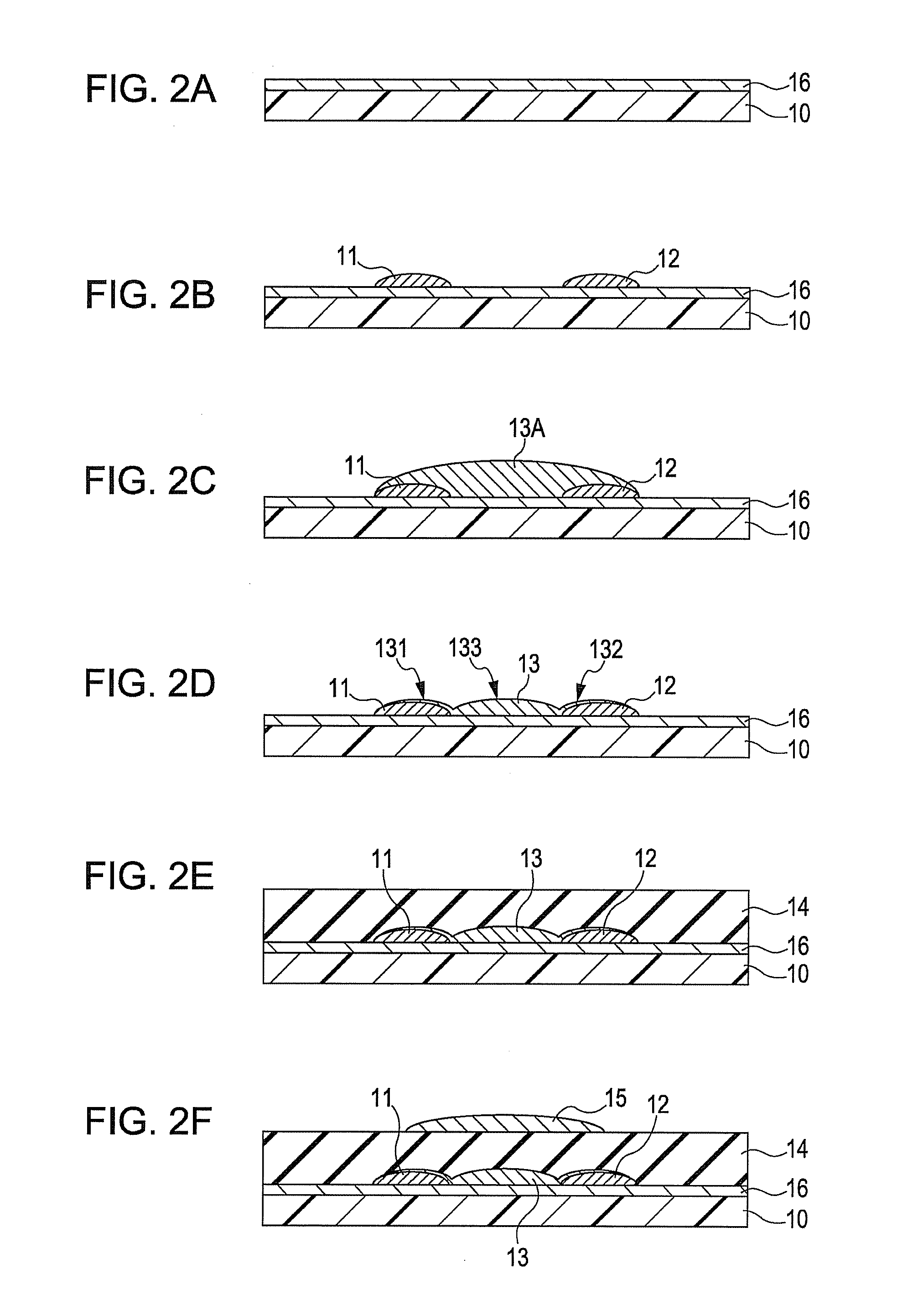
[0016]According to another aspect of the invention, a method for manufacturing an organic transistor is provided. The method includes: forming a source electrode and a drain electrode on a substrate; forming an organic semiconductor layer by applying a solution containing an organic semiconductor across between the source electrode and the drain electrode by an ink jet method and then
drying the solution; forming a gate insulating layer on the organic semiconductor layer; and forming a gate electrode opposing the source electrode and the drain electrode on the gate insulating layer. In forming the organic semiconductor layer, the type of the solution, the conditions of the ink jet method, and the
drying conditions are selected so that the resulting organic semiconductor layer satisfies the relationships W1<W3 and W2<W3, wherein W1 represents the average thickness of a first semiconductor portion of the organic semiconductor layer in a region where the gate electrode and the source electrode oppose each other, W2 represents the average thickness of a second semiconductor portion of the organic semiconductor layer in a region where the gate electrode and the drain electrode oppose each other, and W3 represents the average thickness of a third semiconductor portion of the organic semiconductor layer between the first semiconductor portion and the second semiconductor portion. This method forms the semiconductor layer in such a manner that the third semiconductor portion of the organic semiconductor layer intended to be the channel region has a large thickness while the first semiconductor portion and second semiconductor portion that are to be electrically connected to the source electrode or the drain electrode have small thicknesses. Consequently, the resulting organic transistor can exhibit a superior mobility, on / off ratio and
threshold voltage, and low-dispersion electrical characteristics.
[0017]In this method, selecting the type of the solution, the conditions of the ink jet method, and the
drying conditions means that the type (polarity,
surface tension,
viscosity, solute content, etc), ejection conditions (amount of applied solution,
surface tension of the substrate,
surface shape of the substrate, surface treatment of the substrate,
contact angle of the solution with the substrate, etc), and drying conditions (process temperature,
solvent atmosphere around the solution, pressure, drying technique, etc.) of the solution are set so that the cross sections of the first semiconductor portion, second semiconductor portion and third semiconductor portion of the organic semiconductor layer after drying satisfy the relationships W1<W3 and W2<W3. For example, the organic semiconductor layer having a rising middle portion can be formed by increasing the
viscosity of the solution so as not to flow easily from the middle region to the outer region, or by filling the surroundings with the vapor of the
solvent or selecting a
solvent having a high boiling temperature so that the
vaporization of the solvent can be limited in the outer region.

