Chip-stacked semiconductor device and manufacturing method thereof

a semiconductor and chip technology, applied in semiconductor devices, semiconductor/solid-state device details, electrical devices, etc., can solve the problems of very difficult to flatten the total silicon oxide film, very difficult to meet the requirements of the chip area, and the current silicon etching technique takes a very long time to etch such a narrow (thin) trench, etc., to achieve the effect of increasing the etching rate, reducing the chip area, and reducing the width of the insulation film becoming a

Inactive Publication Date: 2008-10-02
LONGITUDE LICENSING LTD
View PDF1 Cites 29 Cited by
  • Summary
  • Abstract
  • Description
  • Claims
  • Application Information

AI Technical Summary

Benefits of technology

[0016]According to the present invention, the silicon film within the isolation trench can be substantially regarded as a part of the silicon substrate. Therefore, even when the width of t...

Problems solved by technology

However, a forming method of the isolation trench by the conventional technique has the following problems.
However, the current silicon etching technique takes a very long time to etch such a narrow (thin) trench,...

Method used


Image

  • Chip-stacked semiconductor device and manufacturing method thereof
  • Chip-stacked semiconductor device and manufacturing method thereof
  • Chip-stacked semiconductor device and manufacturing method thereof

Examples


Embodiment Construction

[0044]Preferred embodiments of the present invention will now be explained below in detail with reference to the accompanying drawings.

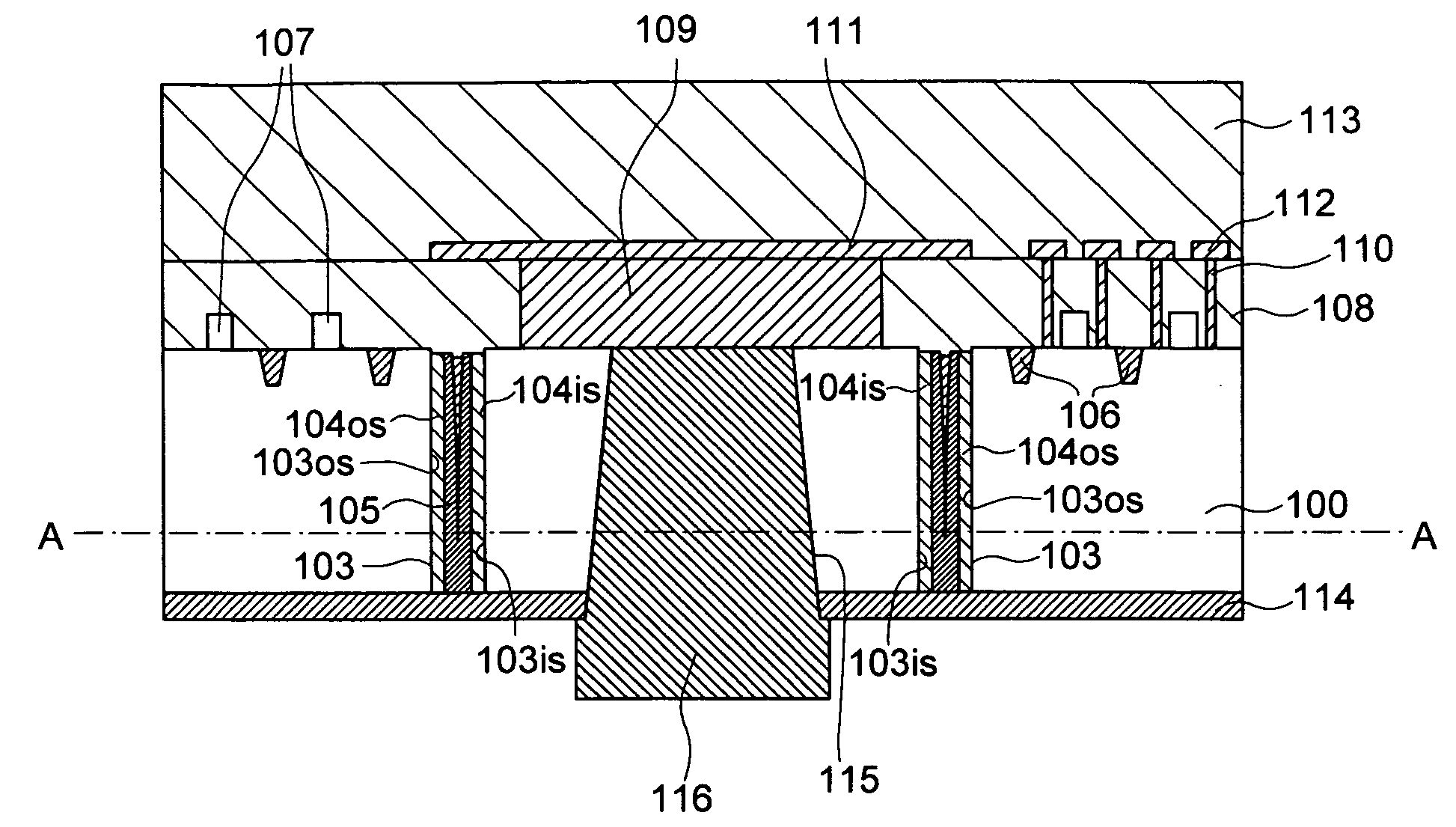
[0045]FIG. 1 to FIG. 13 are process views schematically showing a manufacturing process of a semiconductor device according to a first embodiment of the present invention. FIG. 1 to FIG. 13 show cross-sectional views of an area where one of plural through electrodes to be formed on a silicon substrate is formed and show a peripheral part thereof.

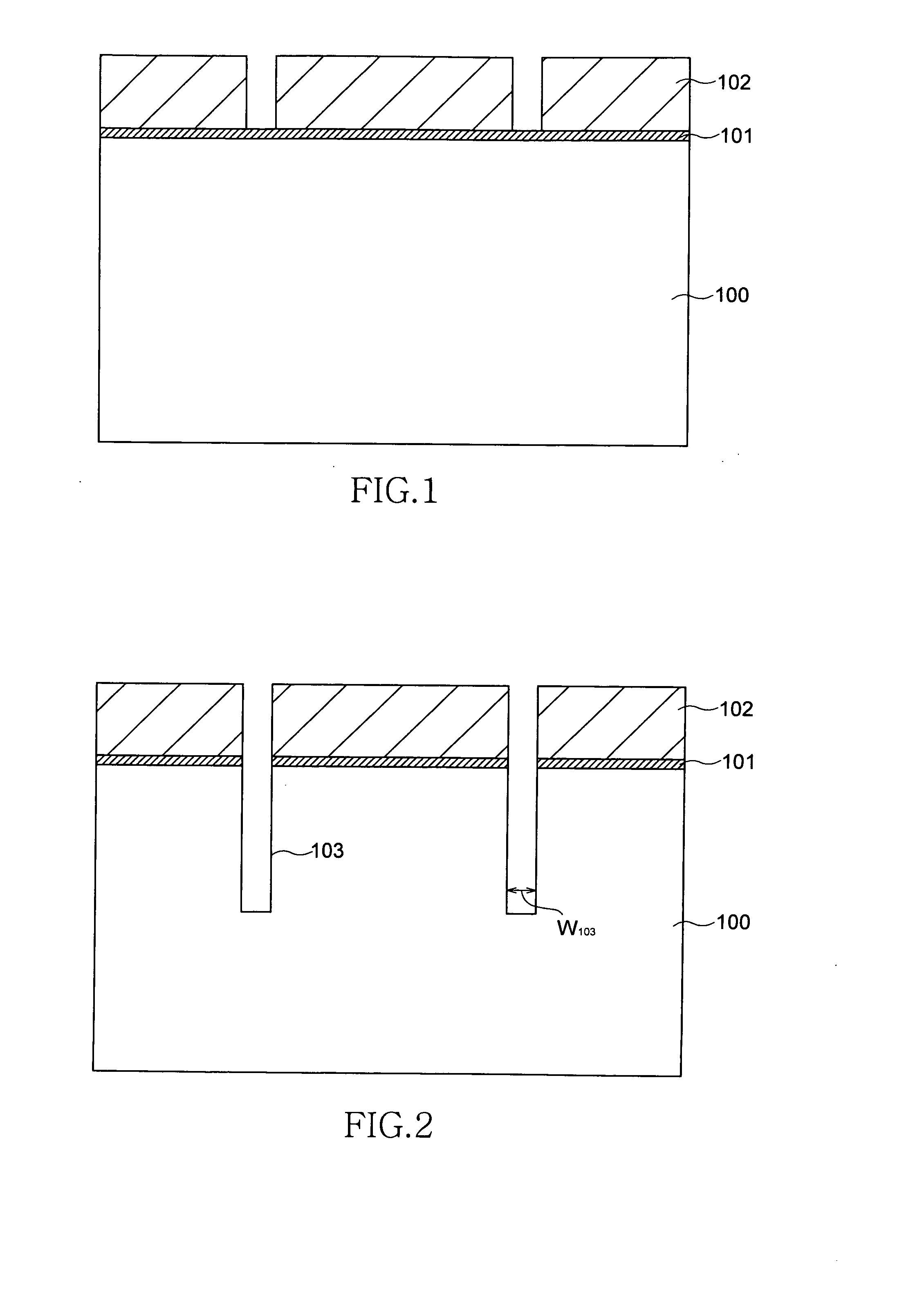
[0046]As shown in FIG. 1, first, the silicon nitride film 101 is formed on a silicon substrate 100, as an oxidation protection film in a later thermal oxide process. Next, the mask layer 102 made of photoresist is formed on the silicon nitride film 101. The mask layer 102 includes an opening to form a ring-shaped isolation trench.

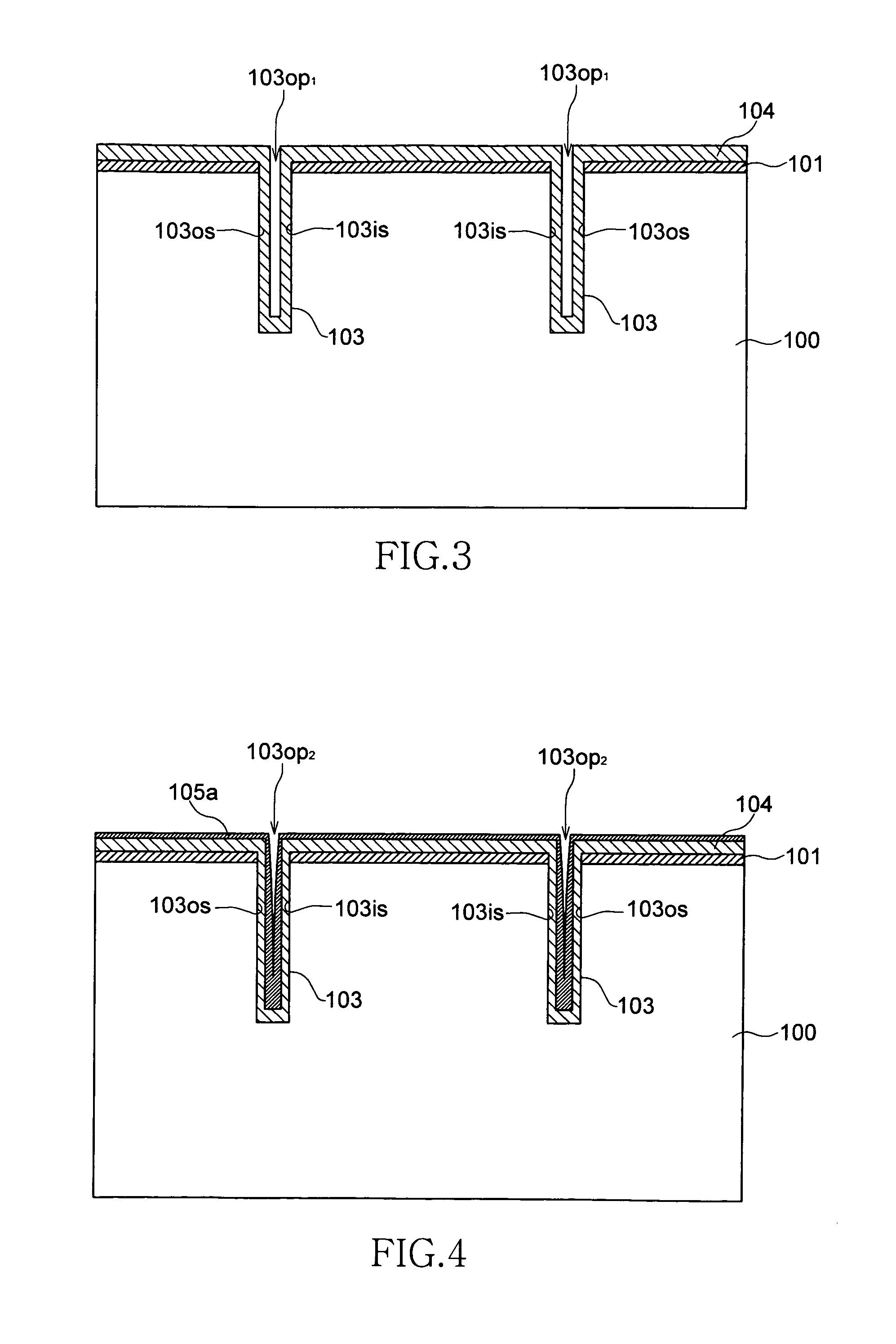
[0047]Next, as shown in FIG. 2, the silicon nitride film 101 and the silicon substrate 100 are etched, using the mask layer 102. As a result, a ring-shaped isolation trench 103 havin...


PUM


Abstract

The semiconductor device according to the present invention includes a through electrode that penetrates through a silicon substrate, an isolation trench provided to penetrate through the silicon substrate to surround the through electrode, a silicon film in contact with an inner surface of the isolation trench, a silicon film in contact with an outer surface of the isolation trench, and an insulation film provided between the silicon films. According to the present invention, the silicon film within the isolation trench can be substantially regarded as a part of the silicon substrate. Therefore, even when the width of the isolation trench is increased to increase the etching rate, the width of the insulation film becoming a dead space can be made sufficiently small. Consequently, the chip area can be decreased.

Description

TECHNICAL FIELD[0001]The present invention relates to a semiconductor device and a manufacturing method thereof, and, more particularly relates to a chip-stacked semiconductor device and a manufacturing method thereof.BACKGROUND OF THE INVENTION[0002]In recent years, a chip-stacked semiconductor device having a plurality of semiconductor chips stacked is proposed. In the chip-stacked semiconductor device, through electrodes that penetrate through a silicon substrate are formed on each semiconductor chip stacked. The semiconductor chips are electrically connected to each other via the through electrodes.[0003]FIGS. 25A and 25B are explanatory views showing a conventional chip-stacked semiconductor device, where FIG. 25A is a schematic cross-sectional view of one through electrode out of plural through electrodes provided on each semiconductor chip, and FIG. 25B shows a cross-sectional view along B-B line of FIG. 25A.[0004]As shown in FIG. 25A, a silicon substrate 10 is formed with a ...

Claims


Application Information

Patent Timeline
IPC IPC(8): H01L23/522H01L21/762H01L21/768
CPCH01L21/76264H01L21/76898Y10S438/977H01L2924/0002H01L2924/00
Inventor UCHIYAMA, SHIRO
Owner LONGITUDE LICENSING LTD
Why Eureka
Try Eureka