Multi-channel semiconductor integrated circuit

a semiconductor and integrated circuit technology, applied in the direction of pulse automatic control, oscillator generator, pulse technique, etc., can solve the problems of device breaking and chip area increasing, and achieve the effect of suppressing chip area increase and preventing device breaking

Inactive Publication Date: 2008-10-09
PANASONIC SEMICON SOLUTIONS CO LTD
View PDF4 Cites 11 Cited by
  • Summary
  • Abstract
  • Description
  • Claims
  • Application Information

AI Technical Summary

Benefits of technology

[0029]Thus, according to the multi-channel semiconductor integrated circuit of the present invention, it is possible to prevent the devic

Problems solved by technology

The conventional high-withstand voltage driver in multi-channel semiconductor integrated circuits has a problem that, when the high-withstand voltage output terminal is short-circuited due to any external factor, the device may be broken, depending on the current overl

Method used


Image

  • Multi-channel semiconductor integrated circuit
  • Multi-channel semiconductor integrated circuit
  • Multi-channel semiconductor integrated circuit

Examples


first embodiment

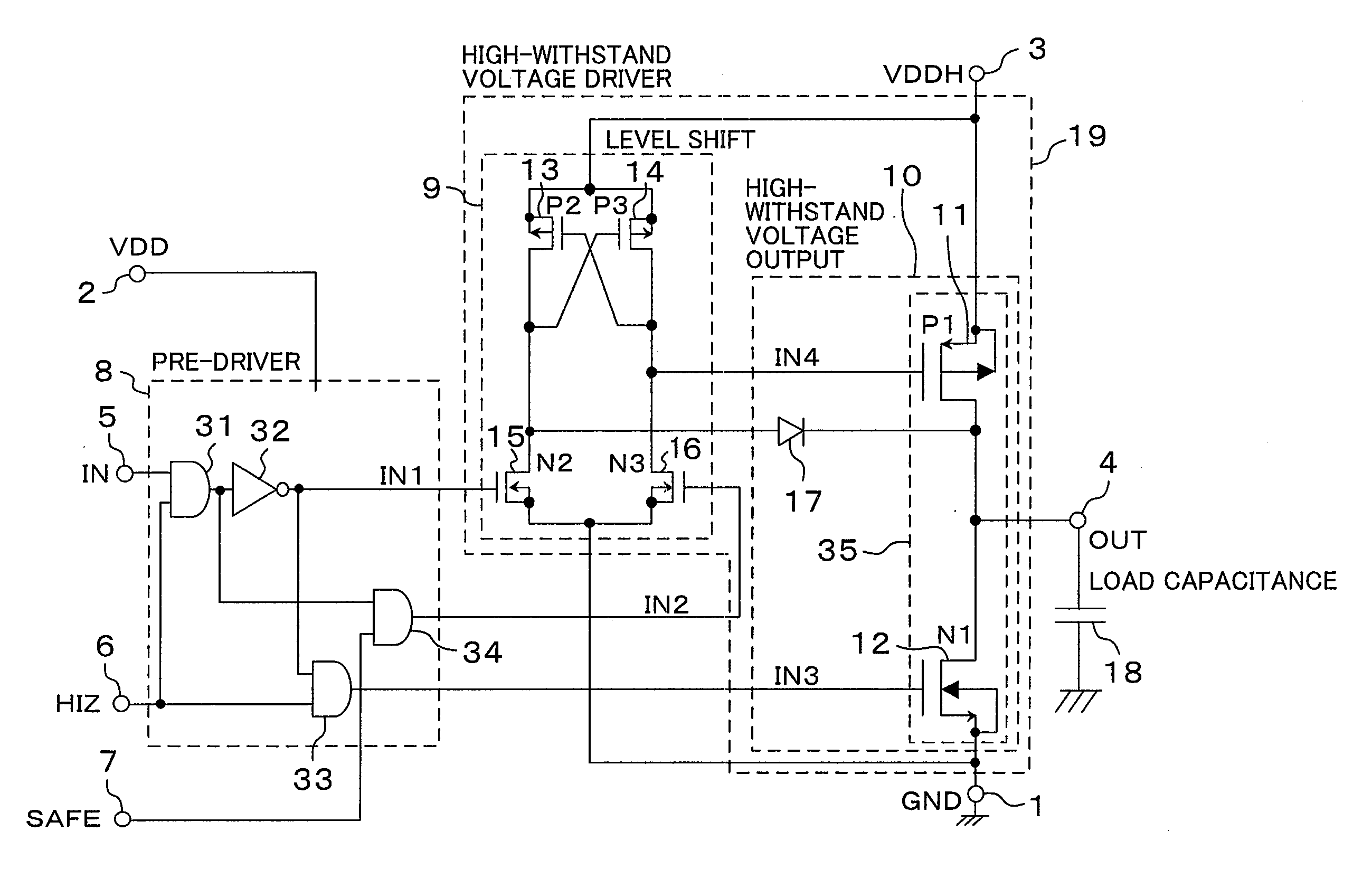
[0038]FIG. 1 is a diagram showing a configuration of a multi-channel semiconductor integrated circuit according to a first embodiment of the present invention.

[0039]As shown in FIG. 1, a high-withstand voltage driver 19 comprises a high-withstand voltage output 10 and a level shift circuit 9. The high-withstand voltage output 10 has a half-bridge 35 including a high-side transistor 11 and a low-side transistor 12. The level shift circuit 9 includes thick-film gate P-type MOS transistors 13 and 14 and thin-film gate N-type MOS transistors 15 and 16. The high-withstand voltage driver 19 is driven by a pre-driver 8 in accordance with a signal which is input through a control input terminal 5 from a low-withstand voltage control section, to charge and discharge a load capacity 18. The high-side transistor 11 and the low-side transistor 12 are forced to be switched OFF, via the pre-driver 8 and the level shift circuit 9, in accordance with a signal which is input through a control input ...

second embodiment

[0053]FIG. 3 is a diagram showing a configuration of a multi-channel semiconductor integrated circuit according to a second embodiment of the present invention.

[0054]As shown in FIG. 3, by incorporating an oscillator 38 as an output protection circuit 20 into the multi-channel semiconductor integrated circuit, an input signal SAFE can be asynchronously input. When the parasitic capacitance is discharged over time, so that the H level cannot be held, or a short-circuit occurs, the state of the high-withstand voltage driver 19 can be reset. Note that an input signal OCR which is input through a terminal 23 is a control signal for the oscillator. The configuration of the built-in oscillator of FIG. 3 is only for illustrative purposes, and the present invention is not limited to this.

third embodiment

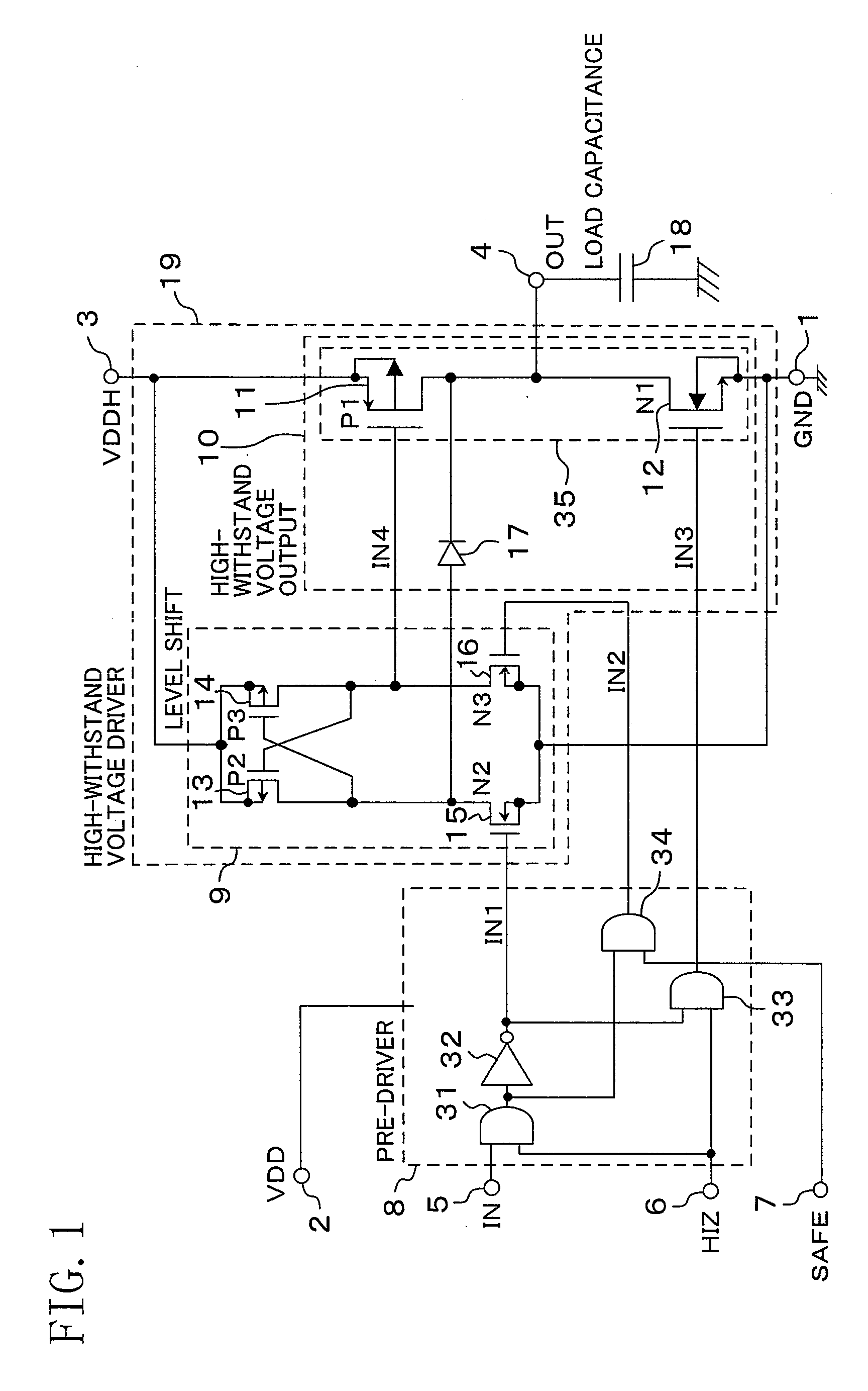
[0055]FIG. 4 is a diagram showing a configuration of a multi-channel semiconductor integrated circuit according to a third embodiment of the present invention.

[0056]As shown in FIG. 4, a high-withstand voltage driver 19 comprises a high-withstand voltage output 10 and a level shift circuit 9. The high-withstand voltage output 10 has a half-bridge 35 including a high-side transistor 11 and a low-side transistor 12. The level shift circuit 9 includes thick-film gate P-type MOS transistors 13 and 14 and thin-film gate N-type MOS transistors 15 and 16. The high-withstand voltage driver 19 is driven by a pre-driver 8 in accordance with a signal which is input through a control input terminal 5 from a low-withstand voltage control section, to charge and discharge a load capacity 18. The high-side transistor 11 and the low-side transistor 12 are forced to be switched OFF, via the pre-driver 8 and the level shift circuit 9, in accordance with a signal which is input through a control input ...


PUM


Abstract

A semiconductor integrated circuit includes a high-side transistor, a low-side transistor, a level shift circuit for driving the high-side transistor, and a pre-driver circuit for driving the low-side transistor. A connection point of the high-side transistor and the low-side transistor serves as an output terminal. The level shift circuit has first and second N-type MOS transistors whose gates are driven by the pre-driver circuit. The semiconductor integrated circuit further includes a diode whose anode is connected to the drain of the first or second N-type MOS transistor to which the gate of the high-side transistor is not connected, and whose cathode is connected to the output terminal.

Description

BACKGROUND OF THE INVENTION[0001]1. Field of the Invention[0002]The present invention relates to a semiconductor integrated circuit and, more particularly, to a multi-channel semiconductor integrated circuit for driving a capacitive load, such as particularly a plasma display or the like.[0003]2. Description of the Related Art[0004]As a conventional high-withstand voltage driver circuit, there is a known half-bridge circuit including a P-channel MOS transistor and an N-channel MOS transistor (see, for example, FIG. 5 in Japanese Unexamined Patent Application Publication No. 2006-94301).[0005]FIG. 6 is a diagram showing a circuit configuration of a conventional drive circuit which is often used as a scanning driver circuit for plasma display panel (PDP) apparatuses.[0006]In FIG. 6, a high-withstand voltage driver 19 comprises a high-withstand voltage output 10 including a high-side transistor 11 and a low-side transistor 12, and a level shift circuit 9 for driving the high-side trans...

Claims


Application Information

Patent Timeline
IPC IPC(8): H03L5/00H03K19/094H03K17/08H03K17/687
CPCH03K3/35613
Inventor HISHIKAWA, NAOKIMATSUNAGA, HIROKIKANEDA, JINSAKU
Owner PANASONIC SEMICON SOLUTIONS CO LTD
Why Eureka
Try Eureka