Light Emitting Device and Method of Manufacturing the Same

a technology of light emitting devices and manufacturing methods, which is applied in the direction of semiconductor/solid-state device manufacturing, semiconductor devices, electrical devices, etc., can solve the problems of low luminous efficiency in which electric energy is converted into light energy, the light is then emitted to the outside of the light emitting device, and the amount of light to be totally reflected is not emitted to the outside but dissipated within, etc., to achieve enhanced light extraction efficiency, high luminous intensity and brightness

Active Publication Date: 2008-10-16
SEOUL VIOSYS CO LTD
View PDF41 Cites 69 Cited by
  • Summary
  • Abstract
  • Description
  • Claims
  • Application Information

AI Technical Summary

Benefits of technology

[0021]In a light emitting device and a method of manufacturing the same according to the present invention, light produced from a side surface of a semiconductor layer, which is not perpendicular to but inclined at a predetermined slop from a horizontal plane, is not totally reflected but emitted to the outside of the light emitting device. Therefore,

Problems solved by technology

Then, a considerable amount of light to be totally reflected is not emitted to the outside but dissipated within the light emitting device due to the internal reflection.
That is, t

Method used


Image

  • Light Emitting Device and Method of Manufacturing the Same
  • Light Emitting Device and Method of Manufacturing the Same
  • Light Emitting Device and Method of Manufacturing the Same

Examples


first embodiment

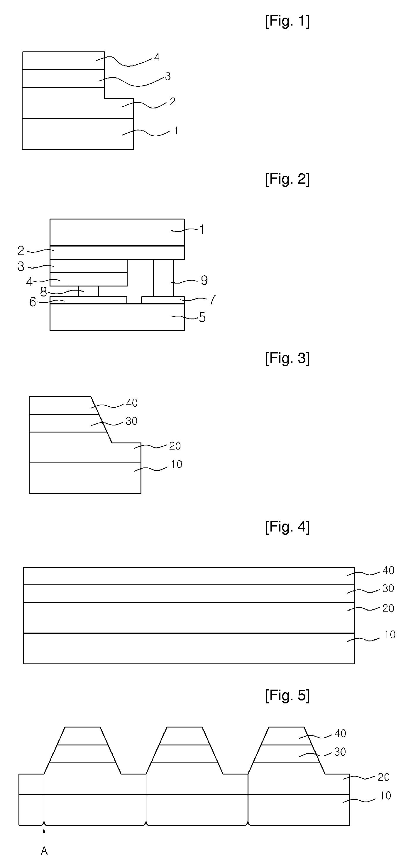
[0037]FIGS. 4 and 5 are sectional views illustrating a process of manufacturing a light emitting device according to the present invention.

[0038]Referring to FIG. 4, an N-type semiconductor layer 20, an active layer 30 and a P-type semiconductor layer 40 are sequentially formed on a substrate 10.

[0039]The substrate 10 refers to a general wafer used for fabricating a light emitting device and is made of at least any one of Al2O3, SiC, ZnO, Si, GaAs, GaP, LiAl2O3, BN, AlN and GaN. In this embodiment, a crystal growth substrate made of sapphire is used.

[0040]A buffer layer (not shown) may be further formed on the substrate 10 to reduce lattice mismatch between the substrate 10 and the subsequent layers upon growth of crystals. The buffer layer may contain GaN or AlN that is a semiconductor material.

[0041]The N-type semiconductor layer 20 is a layer in which electrons are produced and is preferably made from GaN doped with N-type impurities. However, the N-type semiconductor layer 20 is...

second embodiment

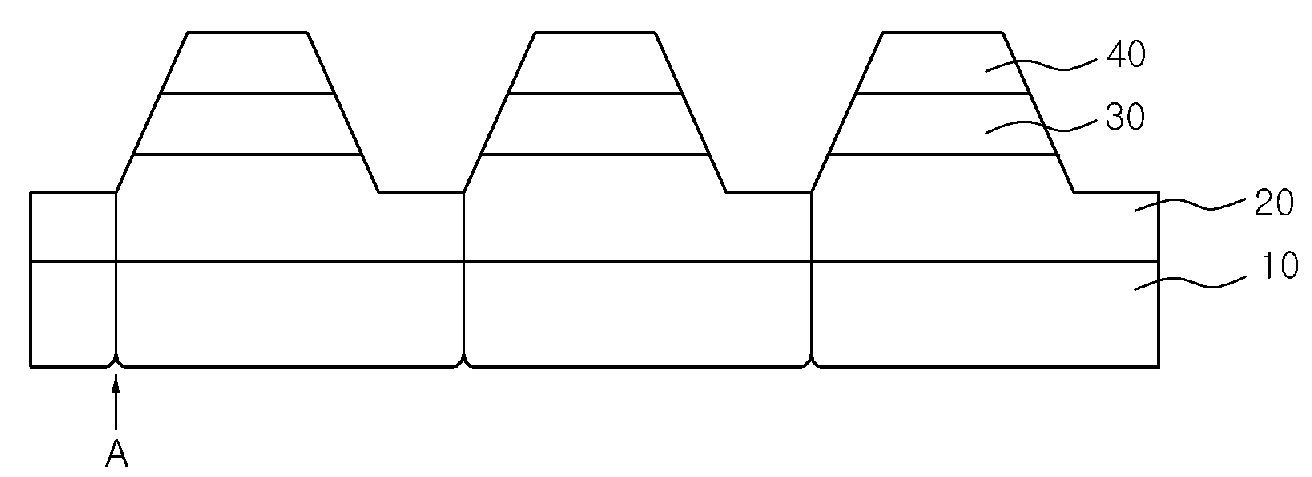
[0055]FIGS. 6 to 7 are sectional views illustrating a process of manufacturing a light emitting device according to the present invention.

[0056]The second embodiment of the present invention is almost the same as the first embodiment. In the second embodiment, however, there is provided a light emitting device in which a plurality of light emitting cells are connected in series, parallel or series-parallel in a wafer level to reduce the size of the device, and they can be driven at proper voltage and current to be used for illustration purpose and can also be driven even with an AC power source. Descriptions overlapping with the previous embodiment will be omitted herein.

[0057]Referring to FIG. 6, an N-type semiconductor layer 20, an active layer 30 and a P-type semiconductor layer 40 are sequentially formed on a substrate 10 through various deposition methods including MOCVD (Metal Organic Chemical Vapor Deposition), CVD (Chemical Vapor Deposition), PCVD (Plasma-enhanced Chemical V...

third embodiment

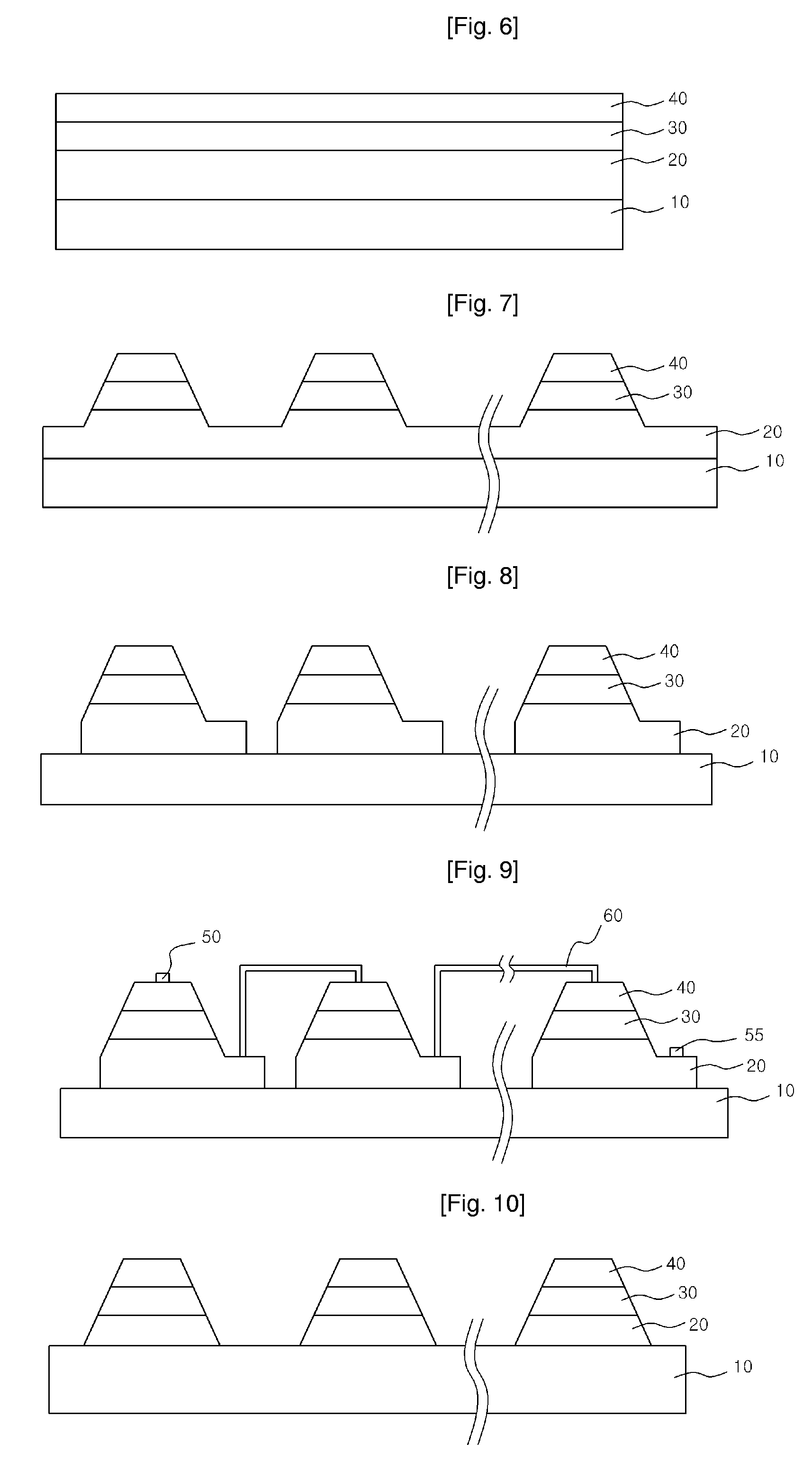
[0067]FIGS. 10 to 13 are sectional views illustrating a process of manufacturing a light emitting device according to the present invention.

[0068]The third embodiment is almost the same as the second embodiment. In the second embodiment, the N-type semiconductor layer 20 is first exposed and a portion of the exposed N-type semiconductor layer 20 is then removed to separate the light emitting cells from one another. In the third embodiment, however, a plurality of light emitting cells are first separated, and a portion of an N-type semiconductor layer 20 is then exposed. Descriptions overlapping with the previous embodiments will be omitted herein.

[0069]Referring to FIG. 10, portions of an N-type semiconductor layer 20, an active layer 30 and a P-type semiconductor layer 40, which are sequentially formed on a substrate 10, are removed to form a plurality of light emitting cells. To this end, after a photoresist has been applied at a thickness of 3 to 50□ on the P-type semiconductor l...


PUM


Abstract

The present invention relates to a light emitting device and a method of manufacturing the light emitting device. According to the present invention, the light emitting device comprises a substrate, an N-type semiconductor layer formed on the substrate, and a P-type semiconductor layer formed on the N-type semiconductor layer, wherein a side surface including the N-type or P-type semiconductor layer has a slope of 20 to 80° from a horizontal plane. Further, the present invention provides a light emitting device comprising a substrate formed with a plurality of light emitting cells each including an N-type semiconductor layer and a P-type semiconductor layer formed on the N-type semiconductor layer, and a submount substrate flip-chip bonded onto the substrate, wherein the N-type semiconductor layer of one light emitting cell and the P-type semi-conductor layer of another adjacent light emitting cell are connected to each other, and a side surface including at least the P-type semiconductor layer of the light emitting cell has a slope of 20 to 80° from a horizontal plane. Further, the present invention provides a method of manufacturing the light emitting device. Accordingly, there is an advantage in that the characteristics of a light emitting device such as luminous efficiency, external quantum efficiency and extraction efficiency are enhanced and the reliability is secured such that light with high luminous intensity and brightness can be emitted.

Description

TECHNICAL FIELD[0001]The present invention relates to a light emitting device and a method of manufacturing the same. More particularly, the present invention relates to a nitride based semiconductor light emitting device with enhanced luminous efficiency and brightness and a method of manufacturing the light emitting device.BACKGROUND ART[0002]A light emitting device refers to an element in which minority carriers (electrons or holes) injected using a p-n junction structure of a semiconductor are produced and certain light is emitted due to recombination of the carriers. A light emitting source is formed from any one or combination of compound semiconductor materials such as GaAs, AlGaAs, GaN, InGaN and AlGaInP, so that a variety of colors can be implemented. For example, a red light emitting device may be formed from GaAsP or the like; a green light emitting device may be formed from GaP, InGaN or the like; a blue light emitting device may be formed using an InGaN / GaN double heter...

Claims


Application Information

Patent Timeline
IPC IPC(8): H01L33/00H01L33/06H01L33/20H01L33/32
CPCH01L27/153H01L33/20H01L33/44H01L33/24H01L33/385H01L33/08H01L2224/48095H01L2224/48137H01L2224/45144H10K59/17H10K50/844H01L2924/00H01L27/15H01L33/28H01L33/32H01L33/62H01L2933/0066
Inventor LEE, JONG LAMLEE, JAE HOYOON, YEO JINHWANG, EU JINKIM, DAE WON
Owner SEOUL VIOSYS CO LTD
Why Eureka
Try Eureka