Target material for electrode film, methods of manufacturing the target material and electrode film

Inactive Publication Date: 2008-10-16
BEIJING BOE OPTOELECTRONCIS TECH CO LTD
View PDF2 Cites 9 Cited by
  • Summary
  • Abstract
  • Description
  • Claims
  • Application Information

AI Technical Summary

Benefits of technology

[0005]The present invention is made in consideration of the problem in the related art that AlNd alloy is expensive and purification of Nd is difficult. In the embodiments of the present invention, it is to substitute a mixture of rare earth elements RE (RE=La, Ce, Pr, Nd), from which Nd is purified, for Nd in a target material, so as to obtain the target material at a reduced cost. Also, metal Ni can be added into the target material to improve resistance to corrosion and oxidation of the target material. That is, a suitable alloy of Al-RE or Al—Ni-RE is provided instead of AlNd alloy to form a target material, and an electrode film that is used in a semiconductor device can be manufactured with such a target material. The present invention also is to provide a method of manufacturing an electrode film.
[0019]As compared with the related art, the embodiments of the present invention reduce the cost for manufacturing the target material and the electrode film, by substituting Nd which is rare and expensive with RE which is relatively abundant and cheap. According to the present invention, the resistance of the target material and the electrode film to corrosion and oxidation can also be further improved by adding Ni into the target material.
[0020]Also, the Al alloy electrode film according to the embodiment of the present invention for a semiconductor device is deposited by using a magnetron sputtering method. For an electrode film deposited by magnetron sputtering, the alloying elements can be solid-dissolved therein to provide a solid solution strengthening effect, so that the thermal stability is improved as compared with the Al alloy film fabricated with other methods.
[0021]Further, in the Al alloy manufactured according to the embodiments of the present invention, the alloying elements are all in a solid solution state. The annealing process performed subsequently causes all or part of the alloying elements in the solid solution state to segregate among the crystal grains in a form of intermetallic compound, so that the resistivity of the alloy film can be reduced. Thus, the alloy film can satisfy the requirement of low resistivity and high thermal stability by applying a heat treatment after the deposition of the alloy film.

Problems solved by technology

At the same time, in the manufacturing of a large scale integrated circuit, a substrate may not provide sufficient landing area for depositing the interconnection wire necessary for an IC.
However, Au is prevented from being widely used by its poor adhering ability with a substrate and poor etching property as well as expensiveness.
Cu is also prevented from being used by its poor adhering ability with a substrate and poor corrosion resistance.
However, Al has a large disadvantage of insufficient thermal stability.
Such thermal instability brings about the problem that very small protrusions (or “hillocks”) will appear on the surface of the metallic electrode film made of Al during subsequent heat treatment.
As a result, if another insulation film is deposited thereon, the hillock may penetrate the insulating film above it and cause a short circuit.
However, due to the fact that the alloying element Nd is a mixture of rare earth elements element, the reserve of which is very small in the earth, and is difficult to purify, and therefore the cost of AlNd is quite high.

Method used


Image

  • Target material for electrode film, methods of manufacturing the target material and electrode film
  • Target material for electrode film, methods of manufacturing the target material and electrode film

Examples


embodiment 1

[0039]Powders of Al, Ni and RE with a purity of 99.99 wt % are sufficiently mixed, and then heated by an induction furnace or a resistance furnace. After the material is completely molten, the molten alloy is atomized into droplets by ejecting working gas (typically Ar or N2 gas) with an atomizing nozzle, and is brought by a flow of the working gas to move quickly toward a cold substrate that is rotating at a certain speed, so as to form a blank of a certain density (typically about 95% of the theoretical density) on a surface of the substrate. The blank is preliminarily reshaped, thermal isostatic pressing densitified, and then formed into a final dimension for a target material through forging and machining.

embodiment 2

[0040]Powders of Al, Ni and RE, which are sufficiently mixed, are heated by an induction furnace or a resistance furnace. After the material is totally molten, the liquid state alloy is blended uniformly and then poured into a mold cavity (e.g., a metallic mold or sand mold) preheated to a certain temperature, and left to be cooled to the room temperature. Then the solidified alloy is taken out of the mold cavity and machined into the final dimension for a target material with or without forging.

embodiment 3

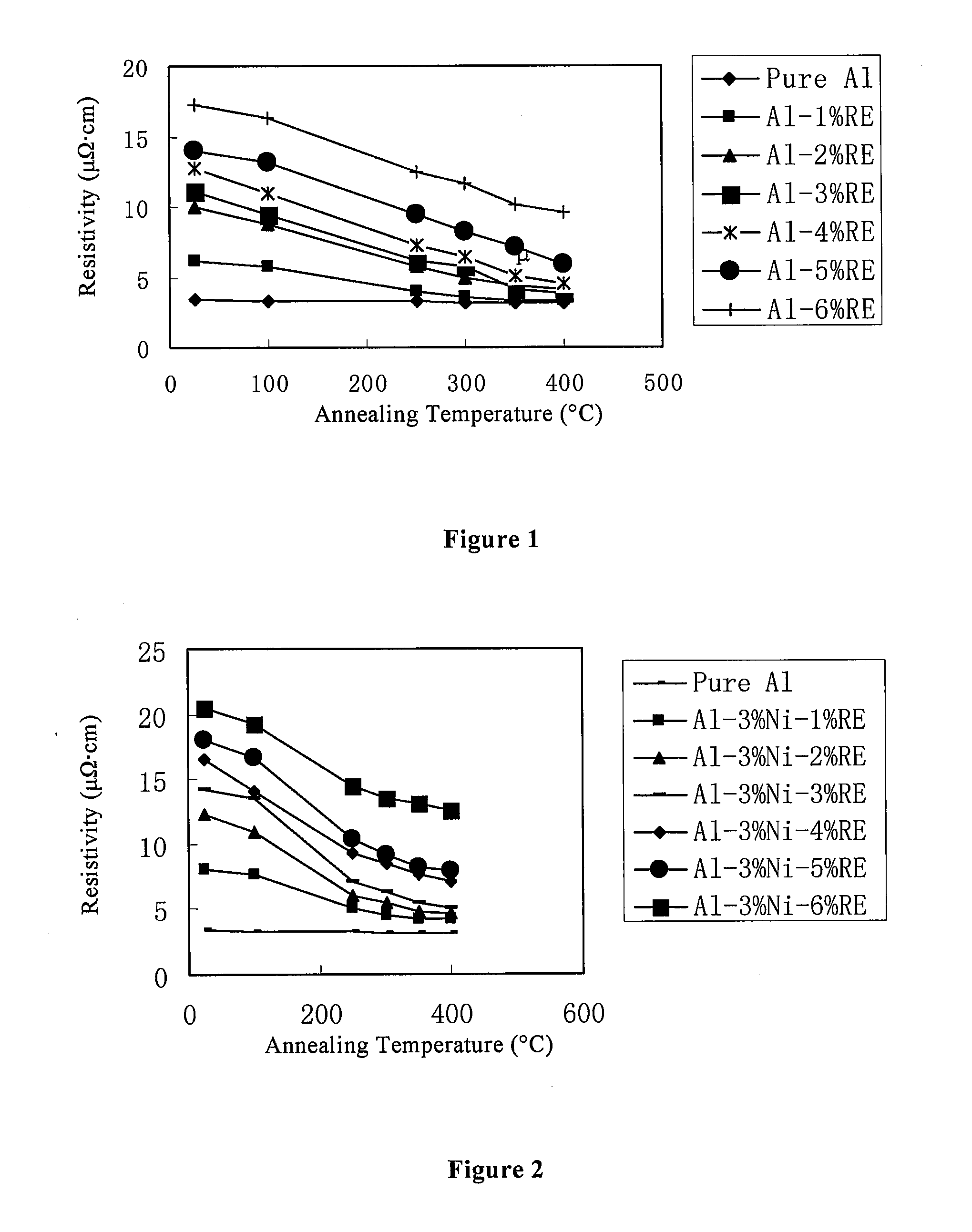
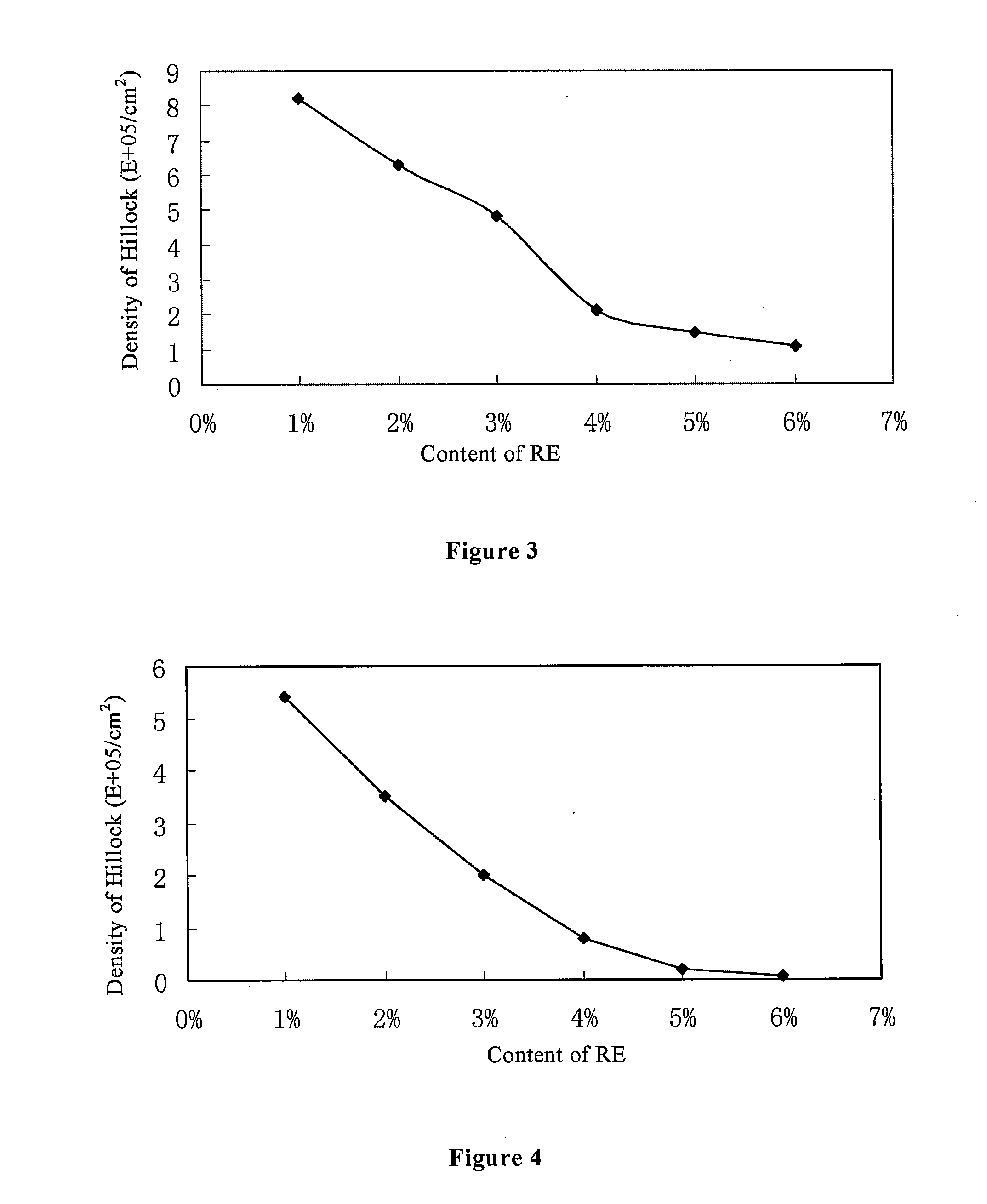
[0041]On a glass plate with a thickness of 0.5 mm, an Al alloy film is deposited to a thickness of about 400 nm by DC magnetron sputtering a target material of Al-RE or Al—Ni-RE alloy. The content of the alloying element(s) except Al in the target material is controlled to be about 1 at %-6 at % during manufacturing the target material. The resulting film is cooled to the room temperature after it is annealed at a temperature of 100° C., 200° C., 300° C. or 400° C., and measurement of the resistivity is performed on the films annealed at the different temperatures by using a four-point method. The hillock density of the resulting film is also measured. The content of every component of the film is measured by using Inductive Couple Plasma (ICP) method. The test results are shown in FIGS. 1 to 4.

[0042]FIG. 1 illustrates variation of resistivity of the alloy film with respect to different annealing temperatures, for different contents of RE in an Al-RE alloy. With an annealing duratio...


PUM

PropertyMeasurementUnit
Temperatureaaaaaaaaaa
Dimensionaaaaaaaaaa
Refractoryaaaaaaaaaa

Abstract

Provided are a target material for manufacturing an electrode film of a semiconductor device, methods of manufacturing the target material and manufacturing the electrode film. The target material comprises Al-RE alloy or Al—Ni-RE alloy, in which RE is a mixture of rare earth elements comprising La, Ce, Pr, and Nd.

Description

BACKGROUND OF THE INVENTION[0001]The present invention relates to a target material for manufacturing electrodes of a semiconductor device, a method of manufacturing the target material, and a method of manufacturing an electrode with the target material. In particular, the present invention relates to a target material for manufacturing the electrode film of a thin-film transistor liquid crystal display (TFT LCD), a method of manufacturing the target material, and a method of manufacturing an electrode with the target material.[0002]At present, as the thin-film transistor liquid crystal display is being developed toward that of large scale and high resolution, metal electrode film with very low electrical resistivity is required for the gate, source and drain electrode of a TFT. For a TFT LCD of over 10 inches, for example, the electrical resistivity of an electrode has to be smaller than 20 μΩcm. At the same time, in the manufacturing of a large scale integrated circuit, a substra...

Claims


Application Information

Patent Timeline
IPC IPC(8): C22C21/00B22D23/00B22D29/00B05D5/12C21D1/26C23C14/34
CPCB22D21/007C23C14/16C23C14/3414H01L29/458H01L29/4908
Inventor XUE, JIANSHELIANG, KE
Owner BEIJING BOE OPTOELECTRONCIS TECH CO LTD
Why Eureka
Try Eureka