Method for manufacturing SOI substrate

a technology of soi substrate and manufacturing method, which is applied in the direction of basic electric elements, electrical apparatus, and semiconductor devices, can solve the problems of different electrical characteristics (resistance) of the silicon layer of the obtained soi substrate from those at the initial stage, and achieve the effect of sufficiently slowing down the cooling rate of the heat treatment process for manufacturing the soi substra

Active Publication Date: 2008-10-16
SHIN ETSU CHEM IND CO LTD
View PDF6 Cites 11 Cited by
  • Summary
  • Abstract
  • Description
  • Claims
  • Application Information

AI Technical Summary

Benefits of technology

[0012]In the present invention, since the single-crystal silicon substrate having the interstitial oxygen concentration which is equal to or below a predetermined concentration is used when manufacturing the SOI substrate by a bonding method, generation of defects (oxygen donors) due to electrically active interstitial oxygen can be considerably suppressed in a process for manufacturing the SOI substrate as well as a process for manufacturing a device.
[0013]Furthermore, since such a substrate is used, a cooling rate of a heat treatment performed in the process for manufacturing the SOI substrate can be sufficiently slowed, and there is no worry about a breakage failure, e.g., a crack or a chip of the substrate due to a thermal strain.

Problems solved by technology

For example, in a case where a heat treatment at approximately 500° C. or above is required in a process for manufacturing an SOI substrate like the above-explained SOITEC method (the SmartCut method), a so-called “new donor” is produced when this heat treatment is carried out in a temperature range of 600 to 700° C., and a so-called “thermal donor” is produced when this heat treatment is performed in a temperature range of 400 to 500° C. These defects (oxygen donors) results in a problem that electrical characteristics (a resistivity) of a silicon layer of an obtained SOI substrate become different from those at the initial stage.

Method used


Image

  • Method for manufacturing SOI substrate
  • Method for manufacturing SOI substrate

Examples


embodiment

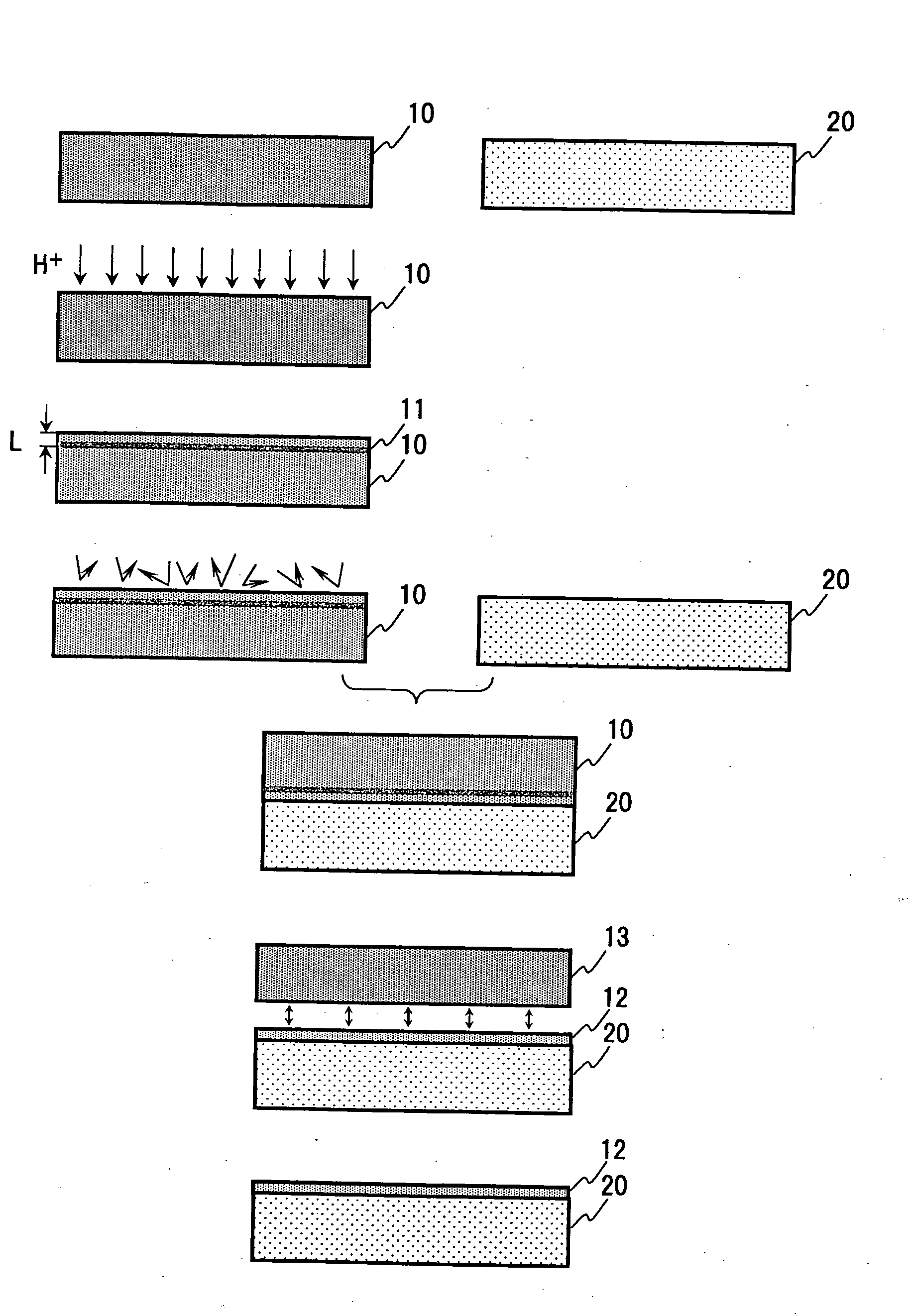
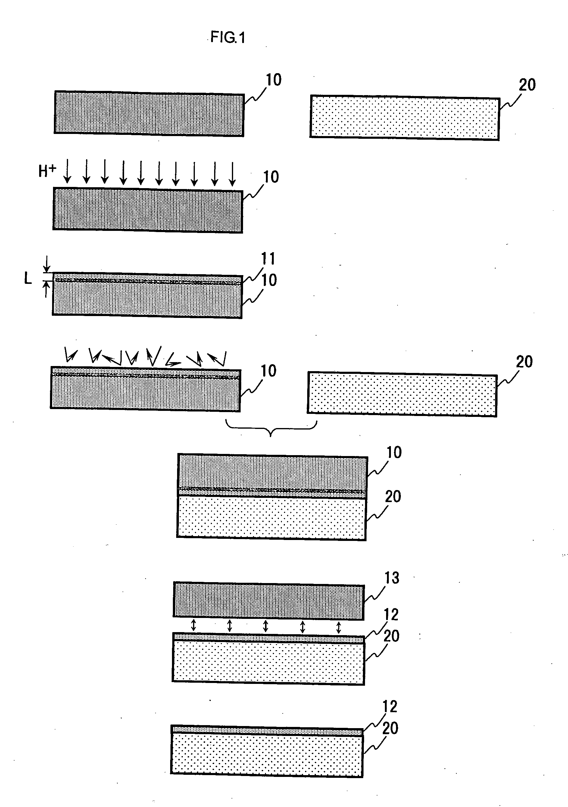
[0016]FIG. 1 are views for explaining a process example of a method for manufacturing an SOI substrate according to the present invention. It is to be noted that an oxide film is not provided on a surface of a silicon substrate in this embodiment, a silicon substrate having an oxide film formed on a surface thereof in advance may be used.

[0017]A silicon substrate 10 depicted in FIG. 1(A) is a p-type (a specific resistance is approximately 10 Ωcm) substrate having a plane orientation (100) and boron (B) doped therein, and it is a single-crystal Si substrate in which an interstitial oxygen concentration measured by infrared absorption spectrophotometry is 1×1018 cm−3 or below. Specifically, the silicon substrate 10 is a substrate with a diameter of 8 inches which has an interstitial oxygen concentration of approximately 5×1017 cm−3 and is grown by an MCZ (magnetic field applied CZ) method. In the present invention, the interstitial oxygen concentration of the single-crystal silicon su...


PUM


Abstract

An SOI substrate having no worry about a fluctuation in electrical characteristics due to generation of oxygen donors is provided.A silicon substrate 10 used for bonding is a single-crystal Si substrate in which an interstitial oxygen concentration measured by infrared absorption spectrophotometry is equal to or below 1×1018 cm−3. The interstitial oxygen concentration of the single-crystal silicon substrate is set to 1×1018 cm−3 or below since a degree of formation of oxygen donors is strongly dependent on the interstitial oxygen concentration. When the interstitial oxygen concentration of the crystal silicon substrate is set to 1×1018 cm−3 or below, a fluctuation in electrical characteristics (a resistivity) of a silicon layer (an SOI layer) of an SOI substrate can be suppressed to a practically problem-free level. Such a single-crystal silicon substrate can be readily obtained by an MCZ method that can control a convection of a silicon melt by applying a magnetic field or an FZ method that uses no quartz crucible.

Description

BACKGROUND OF THE INVENTION[0001]1. Field of the Invention[0002]The present invention relates to a method for manufacturing an SOI substrate having a silicon thin film on a transparent insulative substrate.[0003]2. Description of the Related Art[0004]An SOI (Silicon on Insulator) wafer having a single-crystal silicon (Si) layer on an insulator film such as an oxide film is used as a device forming substrate for the purpose of forming an MOS transistor which is superior in radiation-proof characteristics or latch-up characteristics and also superior in suppression of a short-channel effect. Among others, a low-defect SOI substrate obtained by applying a bonding technology attracts attention. Further, in recent years, using such an SOI substrate as an optical device manufacturing substrate has been examined (e.g., Japanese Patent Application Laid-open No. 145438-1999, Japanese Patent Application Laid-open No. 18926-1994, Japanese Patent Application Laid-open No. 163363-1999, Japanese ...

Claims


Application Information

Patent Timeline
Patent Type & Authority Applications(United States)
IPC IPC(8): H01L21/30
CPCH01L21/2007H01L21/76254H01L29/78603
Inventor KAWAI, MAKOTOKUBOTA, YOSHIHIROITO, ATSUOTANAKA, KOICHITOBISAKA, YUUJIAKIYAMA, SHOJI
Owner SHIN ETSU CHEM IND CO LTD
Why Eureka
Try Eureka