Method to fabricate iii-n field effect transistors using ion implantation with reduced dopant activation and damage recovery temperature

a technology of nitride transistors and ion implantation, which is applied in the direction of semiconductor devices, electrical equipment, basic electric elements, etc., can solve the problems of ion implantation not being used extensively in devices, damage to algans, and iii nitride semiconductor materials, etc., and achieve the effect of reducing the activation temperature of dopants

Inactive Publication Date: 2008-10-23
RGT UNIV OF CALIFORNIA
View PDF14 Cites 57 Cited by
  • Summary
  • Abstract
  • Description
  • Claims
  • Application Information

AI Technical Summary

Benefits of technology

[0023]To overcome the limitations in the prior art described above, and to overcome other limitations that will become apparent upon reading and understanding the present specification, the present invention describes structures to reduce dopant activation temperatures for ion implantation in III-N transistors, such as HEMTs, metal epitaxial semiconductor field effect transistors (MESFETs), heterojunction bipolar transistors (HBTs), and optical devices such as lasers and light emitting diodes (LEDs). A method to increase the temperature at which structures can be annealed by annealing in an active nitrogen ambient, for example, in NH3 in a metalorganic chemical vapor deposition (MOCVD) chamber, is also described.

Problems solved by technology

However, ion implantation has not been used extensively in devices made from Group-III nitride semiconductor materials (also known as “III-nitride,”“III-N” or “nitride” semiconductor materials), such as gallium nitride (GaN), aluminum nitride (AlN), aluminum gallium nitride (AlGaN), indium gallium nitride (InGaN), aluminum indium nitride (AlInN), etc., because of the high temperatures that are typically required to activate dopants, and the capping technology which is then necessary to protect device surfaces.
Because this anneal step is near the decomposition temperature of GaN, it must be a short anneal, and may still cause damage to the AlGaN 18 surface if the process is not carefully controlled.
The need to align the gate 24 metal to the source 20 metal edge is a disadvantage because lithography in the proximity of metals tends to perturb the resultant features due to topology changes and reflections of the gate 24 exposure area off the source 22 metal.
If the spacing is too close, the device may short, while if too long, the device may have increased contact resistance.
This is further complicated by multi-finger devices, where an excess in gate-source 24, 22 spacing on one finger results in a deficit in spacing on the next finger.
An added concern with current devices is that the alloyed contacts 20, 22 may form spikes which penetrate the AlGaN layer 18, which results in increased buffer leakage currents.

Method used


Image

  • Method to fabricate iii-n field effect transistors using ion implantation with reduced dopant activation and damage recovery temperature
  • Method to fabricate iii-n field effect transistors using ion implantation with reduced dopant activation and damage recovery temperature
  • Method to fabricate iii-n field effect transistors using ion implantation with reduced dopant activation and damage recovery temperature

Examples


Embodiment Construction

[0028]In the following description of the preferred embodiment, reference is made to the accompanying drawings which form a part hereof, and in which is shown by way of illustration a specific embodiment in which the invention may be practiced. It is to be understood that other embodiments may be utilized and structural changes may be made without departing from the scope of the present invention.

[0029]Technical Description

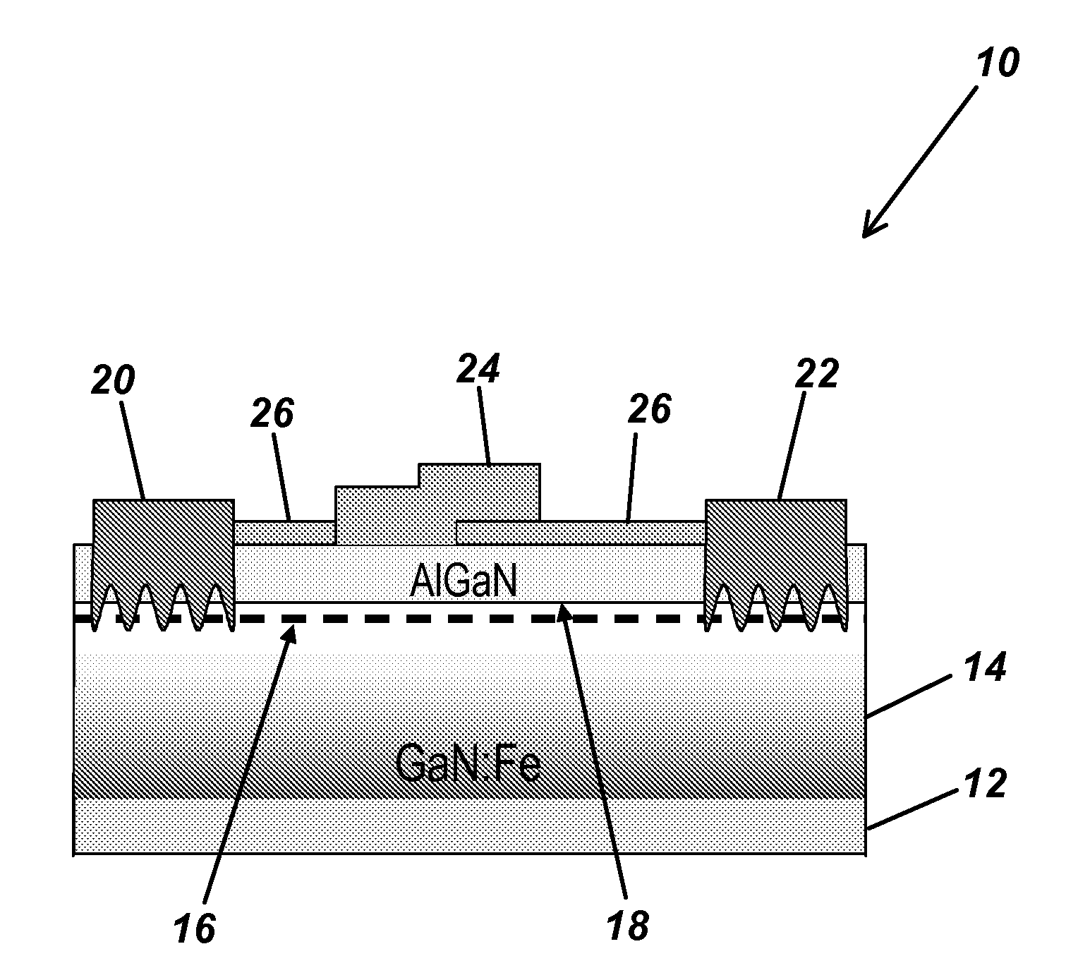
[0030]The present invention describes structures where the channel of an AlGaN / GaN HEMT is designed to reduce the barrier to current flow from implanted GaN regions to the AlGaN / GaN channel.

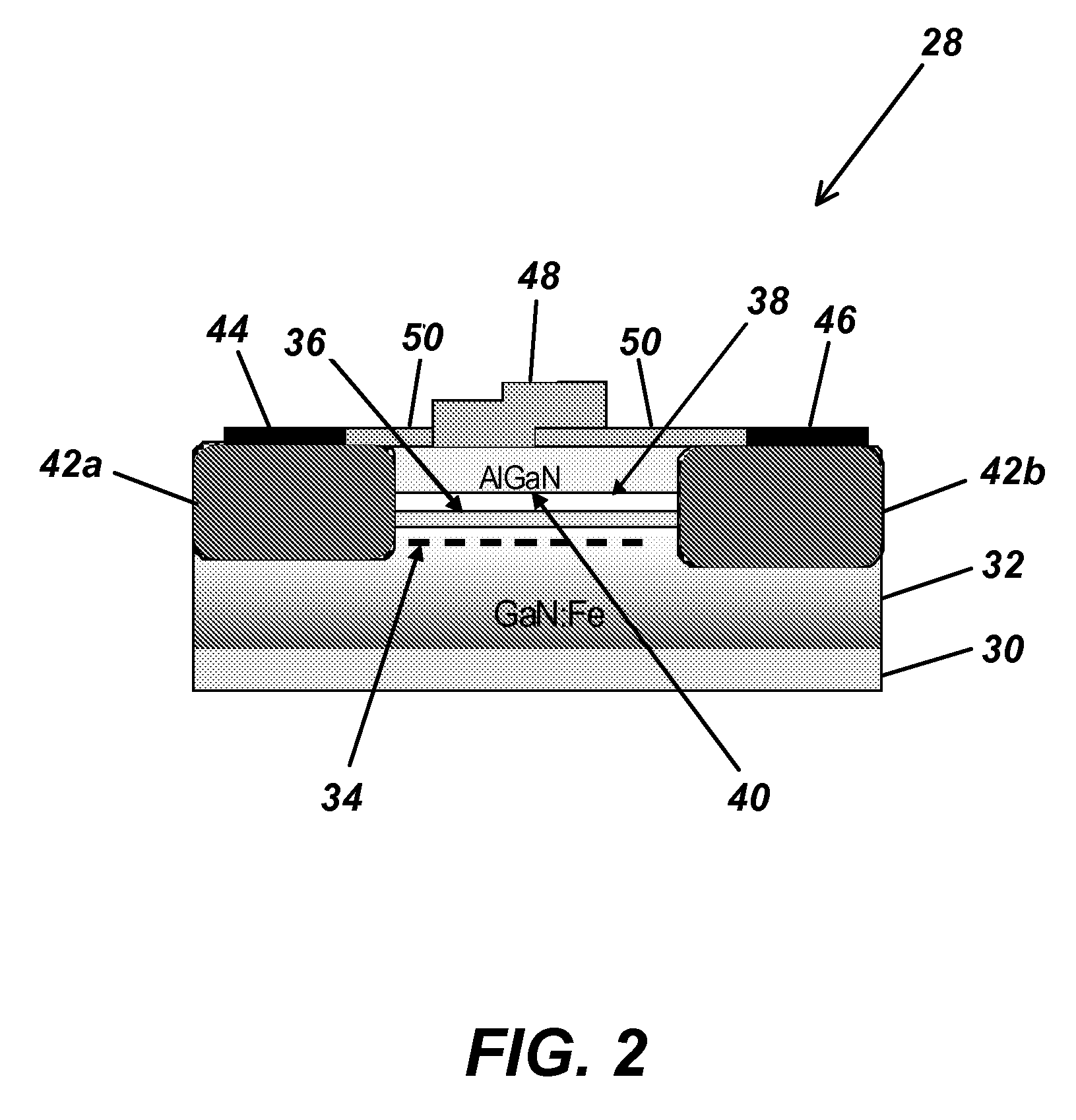
[0031]In a first case, illustrated in the schematic of FIG. 2, the use of ion implantation in conjunction with a GaN spacer HEMT 28 is proposed. The ion implanted gallium-face (Ga-face) AlGaN / GaN HEMT 28 of FIG. 2 includes an SiC substrate 30, a GaN:Fe layer 32, a GaN 2DEG channel 34, an Al(In)N interlayer or barrier layer 36, a GaN spacer layer 38, a GaN or GaN / AlGaN layer 40,...


PUM

PropertyMeasurementUnit
temperaturesaaaaaaaaaa
temperatureaaaaaaaaaa

Abstract

Structures to reduce dopant activation temperatures for ion implantation in III-N transistors, using low aluminum content layers in proximity to the conducting channel, are disclosed. A method to increase the temperature at which structures can be annealed by annealing in an active nitrogen ambient, for example, in NH3 in a metalorganic chemical vapor deposition (MOCVD) chamber, is also disclosed.

Description

CROSS-REFERENCE TO RELATED APPLICATIONS[0001]This application claims the benefit under 35 U.S.C. Section 119(e) of the following co-pending and commonly-assigned U.S. patent application:[0002]U.S. Provisional Patent Application Ser. No. 60 / 894,124, filed on Mar. 9, 2007, by Lee S. McCarthy, Umesh K. Mishra, Felix Recht, and Tomas A. Palacios Gutierrez, entitled “METHOD TO FABRICATE III-N FIELD EFFECT TRANSISTORS USING ION IMPLANTATION WITH REDUCED DOPANT ACTIVATION AND DAMAGE RECOVERY TEMPERATURE,” attorneys' docket number 30794.226-US-P1 (2006-518-1);[0003]which application is incorporated by reference herein.[0004]This application is related to the following co-pending and commonly-assigned applications:[0005]U.S. Utility patent application Ser. No. 10 / 962,911, filed on Oct. 12, 2004, by Likun Shen, Sten J. Heikman and Umesh K. Mishra, entitled “GaN / AlGaN / GaN DISPERSION-FREE HIGH ELECTRON MOBILITY TRANSISTORS,” attorneys docket number 30794.107-US-U1, (2003-177), which application...

Claims


Application Information

Patent Timeline
Patent Type & Authority Applications(United States)
IPC IPC(8): H01L29/778H01L21/338H01L21/263H01L33/00
CPCH01L21/2654H01L21/26546H01L21/26586H01L21/3245H01L29/2003H01L29/207H01L29/66462H01L29/7787H01L33/0095
Inventor MCCARTHY, LEE S.MISHRA, UMESH K.RECHT, FELIXPALACIOS GUTIERREZ, TOMAS APOSTOL
Owner RGT UNIV OF CALIFORNIA
Why Eureka
Try Eureka