Semiconductor device package to improve functions of heat sink and ground shield

a technology of heat sink and semiconductor device, applied in the direction of semiconductor devices, semiconductor/solid-state device details, electrical devices, etc., can solve the problems of affecting the acceptance of wlp, increasing the thickness of the package, increasing the size of the build-up layer, etc., to achieve excellent ground shielding, simple process, and better thermal dissipation

Inactive Publication Date: 2008-10-23
ADVANCED CHIP ENG TECH
View PDF8 Cites 60 Cited by
  • Summary
  • Abstract
  • Description
  • Claims
  • Application Information

AI Technical Summary

Benefits of technology

[0007]Further advantage of the present invention is that a metal layer is provided for achieving better thermal dissipation, especially, for high power device, the present invention provides excellent ground shielding for RF or high frequency device. In one embodiment, the present invention includes a metal layer that is employed as an antenna. The present invention offers the scheme of Package on Package to integrate device and shrink the stacking size with simple process.
[0008]The present invention provides a package structure comprising a substrate having first contact pad, at least one through hole formed therein. A metal layer is formed at lower surface of the substrate, wherein the at least one through hole connects to the metal layer from the first contact pads for heat dissipation and ground shielding. A chip with a bonding pad is attached on the first contact pads by an adhesive with high thermal conductivity. A dielectric layer is formed on the chip and a second contact pad is formed at upper surface of the substrate. A redistribution layer (RDL) is formed above the chip and coupled the bonding pad to the second contact pad for electrical connection. A solder ball formed on the second contact pad formed on upper surface of the substrate.
[0009]The present invention provides a method for manufacturing a package structure, comprising: providing a substrate with a first contact pad, a second contact pad and at least one through hole; dispensing an adhesive on the back side of a chip with a bonding pad; attaching the chip on the first contact pad; forming build up layer to couple the second pad with the boding pad; forming a top protection layer on the chip and the substrate by coating or printing; placing a solder ball on the second contact pad; and reflowing the solder ball whereby forming the solder ball on the second contact pad.

Problems solved by technology

Though the WLP technique has advantages mentioned above, some issues still exist influencing the acceptance of WLP technique.
The build up layer also increases the size of the package.
Therefore, the thickness of the package is increased, which conflict with the demand of reducing the size of a chip.

Method used


Image

  • Semiconductor device package to improve functions of heat sink and ground shield
  • Semiconductor device package to improve functions of heat sink and ground shield
  • Semiconductor device package to improve functions of heat sink and ground shield

Examples


Embodiment Construction

[0015]The invention will now be described in greater detail with preferred embodiments of the invention and illustrations attached. Nevertheless, it should be recognized that the preferred embodiments of the invention is only for illustrating. Besides the preferred embodiment mentioned here, the present invention can be practiced in a wide range of other embodiments besides those explicitly described, and the scope of the present invention is expressly not limited expect as specified in the accompanying Claims.

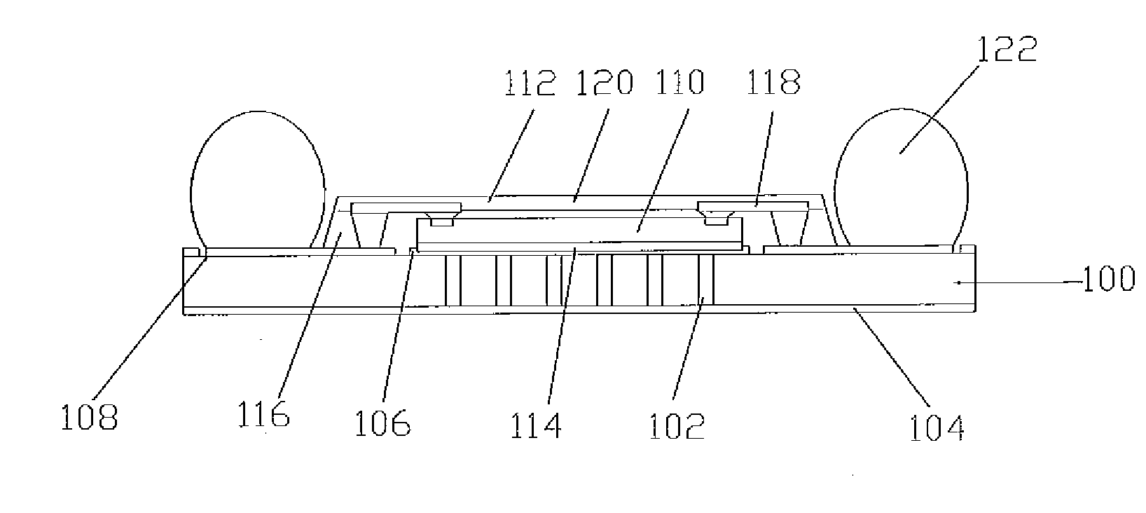
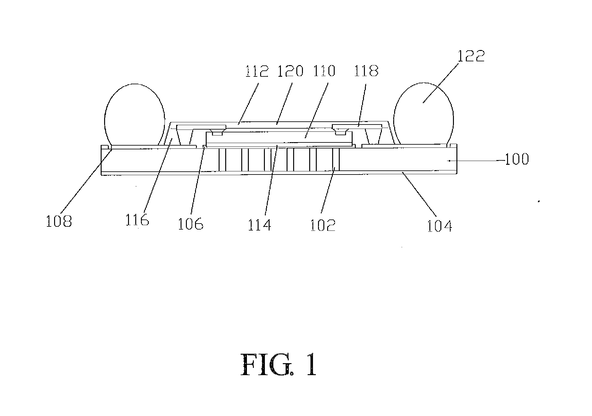
[0016]FIG. 1 illustrates a package structure discloses in one embodiment of the present invention. A substrate 100, preferably, made of FR4 / FR5 / BT or metal / alloy, is provided with through holes 102 formed therein; wherein the through holes 102 are filled with conducting material such as metal, preferably copper material. A conductive layer, for instant metal layer 104, is attached on one surface of the substrate 100 and a conductive (metal) layer 106 is formed on another surfa...


PUM


Abstract

The present invention provides a package structure and a method for forming the same. The structure comprises a substrate with contact pads and through holes filled with conducting metals for performing heat dissipation and ground shielding A chip with bonding pads is attached on the contact pad by an adhesive with high thermal conductivity to achieve heat dissipation. A RDL is formed on the substrate and the chip to couple the bonding pad and the contact pad formed on the substrate. The structure of present invention can improve the thickness thereof, and the heat dissipation and ground shielding of the structure are enhanced. Furthermore, the structure can achieve package on package (PoP) structure.

Description

FIELD OF THE INVENTION[0001]The present invention relates to a structure and a method for semiconductor package, and more particularly to thin semiconductor package.DESCRIPTION OF THE PRIOR ART[0002]In the field of semiconductor devices, the device density is increased continuously; therefore reducing the device dimension is demanding. Chip package technique is highly influenced by the development of integrated circuits, therefore, as the size of electronics has became demanding, so does the package technique. For the reasons mentioned above, the trend of package technique is toward ball grid array (BGA), flip chip (FC-BGA), chip scale package (CSP), Wafer level package (WLP) today; wherein, the structure formed by WLP has extremely small dimension and good electrical properties. By utilizing WLP technique, the manufacturing cost and time is reduced and the resulting structure of WLP can be equal to the chip; therefore, this technique can meet the demands of miniaturization of elect...

Claims


Application Information

Patent Timeline
Patent Type & Authority Applications(United States)
IPC IPC(8): H01L23/12H01L21/00
CPCH01L23/3677H01L23/49816H01L23/5389H01L23/552H01L24/24H01L24/82H01L25/105H01L2223/6677H01L2224/24226H01L2224/73267H01L2924/01015H01L2924/01029H01L2924/01059H01L2924/01075H01L2924/01078H01L2924/01079H01L2924/01082H01L2924/14H01L2924/15311H01L2924/1532H01L2924/15331H01L2924/19043H01L2924/30105H01L2924/3025H01L2924/01006H01L2924/01033H01L2924/014H01L2225/1023H01L2225/1058H01L2225/1094H01L2224/32225H01L2924/00H01L23/06H01L23/08
Inventor YANG, WEN-KUNLIN, DIANN-FANG
Owner ADVANCED CHIP ENG TECH
Why Eureka
Try Eureka