Structure and method for self protection of power device with expanded voltage ranges

a power device and voltage range technology, applied in the direction of semiconductor devices, semiconductor/solid-state device details, electrical apparatus, etc., can solve the problems of unfavorable manufacturing and operation costs, increase in die size, and damage to other components

Inactive Publication Date: 2008-10-30
ALPHA & OMEGA SEMICON LTD
View PDF6 Cites 35 Cited by
  • Summary
  • Abstract
  • Description
  • Claims
  • Application Information

AI Technical Summary

Benefits of technology

[0011]It is therefore an aspect of the present invention to provide a new and improved resettable PTC protection configuration that can

Problems solved by technology

Under high power conditions, the power devices often fail in a “short circuit” condition and that can result in damages to other components in the system where the power devices are implemented.
However, as shown in FIG. 1B such configuration has a limitation that for very high current application, multiple fuses and pads would be required thus causing an increase in die size and that leads to unfavorable cost impacts in manufacturing and in operation.
Another disadvantage associates with multiple fuses and pads is that in case not all fuses blow open during an over-current condition, the active region of the device where the fuse did not blow open would be damaged.
Furthermore, the addition of the protective circuit such as metal fuse, poly-fuse, or other “fail-open” protective circuits, often adversely affects the device or system performance.
The fuse protection also has a disadvantage that such protection is not re-settable, once the fuse is broken, the fuse connection is broken even the over current condition is then eliminated.
When the plastic heats up, it expands, forcing the carbon grains apart, and causing the resistance of the device to rise rapidly.
Even though the application of materials of a positive temperature coefficient (PTC) for over-current protection of electronic devices is well known, there are stil

Method used


Image

  • Structure and method for self protection of power device with expanded voltage ranges
  • Structure and method for self protection of power device with expanded voltage ranges
  • Structure and method for self protection of power device with expanded voltage ranges

Examples


Embodiment Construction

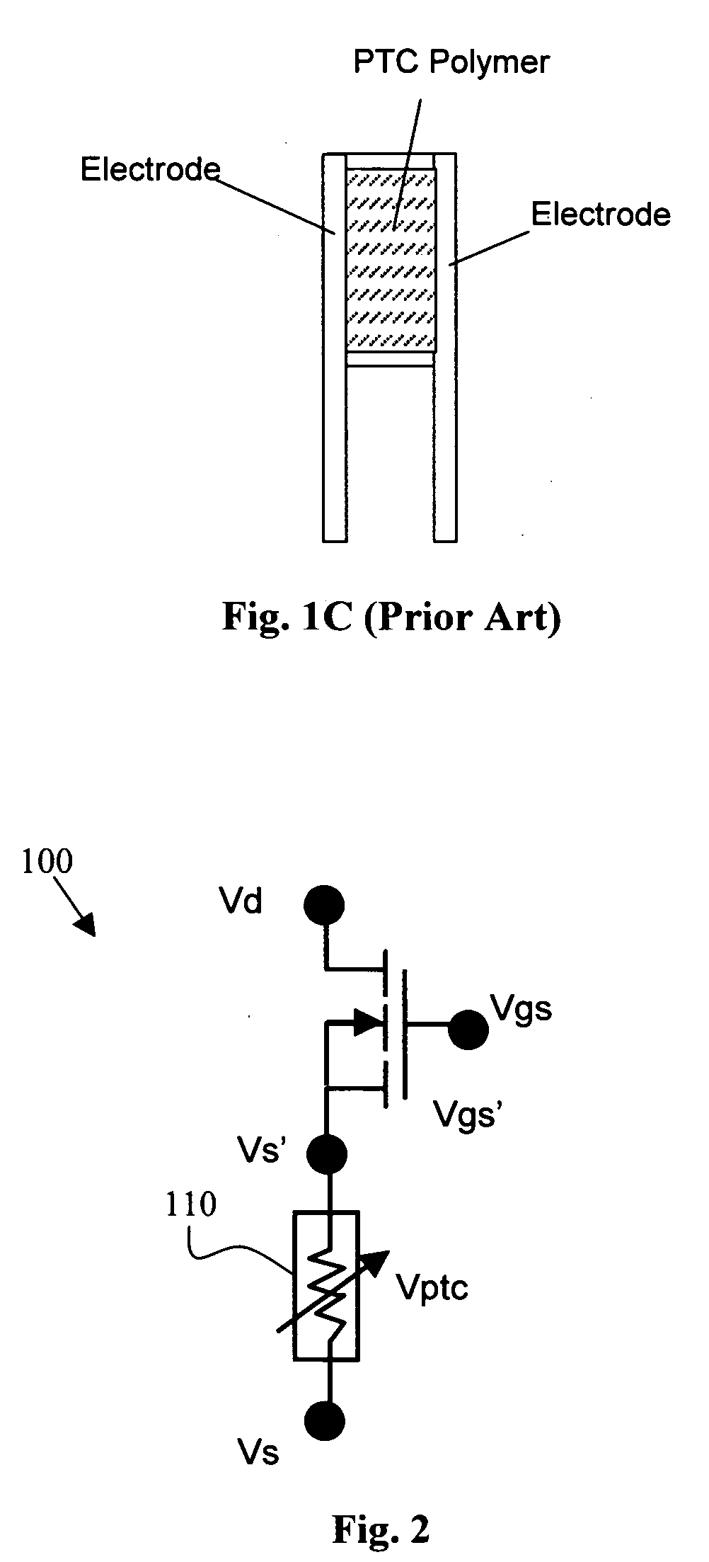
[0029]FIG. 2 is a schematic representation of a PTC protected FET 100, (which can also be referred to as a fuse FET) that includes a resistor 110 composed of a material that has a positive temperature coefficient (PTC) and configured as a conductive layer connected to a source electrode and further provides a feedback voltage to regulate the gate-source voltage. As the temperature of the device under protection is increased, the resistance of the PTC resistor 110 is also increased and the resistance is drastically increased once the PTC trip temperature is reached. In this protection configuration, any source to drain current (Ids) increase will result in a voltage drop Vptc across the PTC structure 110 thus reducing the FET control voltage Vgs. Specifically, the voltages have functional relationships that can be represented as:

Vgs=Vgs′+Vptc

Vgs′=Vgs−Vptc

[0030]When the temperature of the device is above the trip temperature of the PTC, the voltage drop across the PTC structure Vptc...


PUM


Abstract

A vertical semiconductor power device includes a top surface and a bottom surface of a semiconductor substrate constituting a vertical current path for conducting a current there through. The semiconductor power device further includes an over current protection layer composed of a material having a resistance with a positive temperature coefficient (PTC) and the over current protection layer constituting as a part of the vertical current path connected to a source electrode and providing a feedback voltage a gate electrode of the vertical semiconductor power device for limiting a current passing there through for protecting the semiconductor power device at any voltage.

Description

[0001]This application is a Continuation in Part (CIP) Application and claims priority to pending U.S. patent application entitled “STRUCTURE AND METHOD FOR SELF PROTECTION OF POWER DEVICE” filed on Jan. 25, 2007 and accorded Ser. No. 11 / 657,862 by a common Applicant of this Application, the benefit of its filing date being hereby claimed under Title 35 of the United States Code.BACKGROUND OF THE INVENTION[0002]1. Field of the Invention[0003]The invention relates generally to a device configuration and method of protecting the device. More particularly, this invention relates to an improved circuit configuration and method of protecting active devices operated at a high voltage from damages due to over current caused by an electrical short by using a conductive material with a positive temperature coefficient.[0004]2. Description of the Relevant Art[0005]Under high power conditions, the power devices often fail in a “short circuit” condition and that can result in damages to other c...

Claims


Application Information

Patent Timeline
IPC IPC(8): H01L23/62H02H9/00
CPCH01L23/3121H01L2924/1306H01L23/62H01L24/40H01L24/49H01L24/73H01L24/83H01L24/85H01L2224/05644H01L2224/05647H01L2224/05655H01L2224/48247H01L2224/48472H01L2224/4903H01L2224/49051H01L2224/49111H01L2224/73221H01L2224/83801H01L2924/01006H01L2924/01013H01L2924/01015H01L2924/01028H01L2924/01029H01L2924/01056H01L2924/01075H01L2924/01078H01L2924/01079H01L2924/01082H01L2924/13091H01L2924/19043H01L24/48H01L2924/01033H01L2924/014H01L23/3135H01L2924/13062H01L2924/13064H01L2224/85H01L2924/00H01L2924/00012H01L2924/181H01L2924/00014H01L2224/40095H01L2224/40245H01L2224/8385H01L2224/05553H01L2224/0603H01L2224/84801H01L2224/40491H01L24/84H01L2224/45099
Inventor HEBERT, FRANCOIS
Owner ALPHA & OMEGA SEMICON LTD
Why Eureka
Try Eureka