CD-GISAXS System and Method

a technology of cdgisax and system, applied in the field of cdgisaxs system and method, can solve the problems of large degradation of performance, device failure, or manufacturing yield, and limited application of afm, etc., and achieve the effect of ample potential and high measurement accuracy and sensitivity

Active Publication Date: 2008-11-06
CARL ZEISS X RAY MICROSCOPY
View PDF39 Cites 112 Cited by
  • Summary
  • Abstract
  • Description
  • Claims
  • Application Information

AI Technical Summary

Benefits of technology

[0010]X-ray scatterometry provides high measurement accuracy and sensitivity due to its short wavelength, non-destructive capability due to potentially low dosages, ...

Problems solved by technology

Semiconductor devices are very sensitive to these dimensions and even minute variations can lead to large degradations in their performance, device failure, or manufacturing yield.
Other techniques such as atomic force microscopy (AFM) have also been applied to CD measurement, but wide use of AFM, for example, has been limited by its measurement speed and probe size.
The disadvantages of CD-SEM have become more critical: 1) the well known charging problem limits the achievable resolution for IC metrology applications; 2) radiation damage induced dimensional shrinking of resists (note: this is particularly problematic with some 193 nm photoresists, for example, that shrink when exposed to electron beams, leading to “CD slimming”); 3) incompatibility with some low-k dielectrics; and 4) CD-SEM is essentially a surface technique making it difficult to measure 3D profiles.
Similarly, OCD faces a number of fundamental difficulties: (1) its long wavelength is significantly larger than the device feature size and therefore does not p...

Method used


Image

  • CD-GISAXS System and Method
  • CD-GISAXS System and Method
  • CD-GISAXS System and Method

Examples


Embodiment Construction

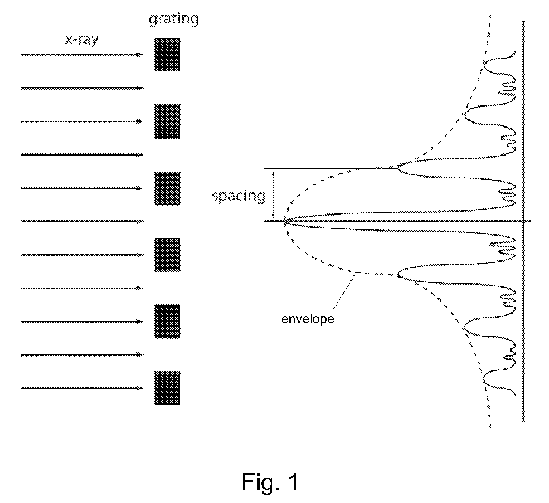
[0022]Theoretical basis for longer wavelengths:

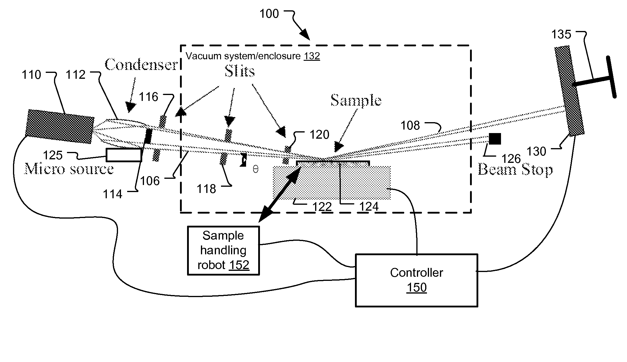
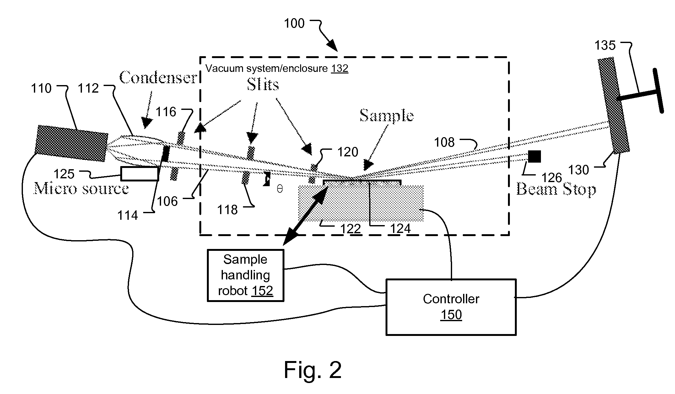
[0023]The three grand metrology challenges all require measuring critical dimensions in 3D of structures with a linear dimension 45 nanometers (nm) or smaller. The measurements are sometimes made within a small area, known as the wafer test pad that is usually located inside the so-called scribe-line along which the chips are separated. The area is typically less than 100 micrometers (μm) on a side but the side along the scribe-line direction can be longer if necessary. For in-line metrology applications, the structures within the test pad are typically repeated periodic structures.

[0024]The throughput of a CD-SAXS system is proportional to both the x-ray flux incident on the test pad and the scattering strength (fraction of the incident x-rays scattered) by the structure within the test pad. Therefore, to improve the throughput of CD-SAXS with the problem as defined above, one needs to improve and optimize both of those parameters.

[002...


PUM


Abstract

CD-GISAXS achieves reduced measurement times by increasing throughput using longer wavelength radiation (˜12×, for example) such as x-rays in reflective geometry to increase both the collimation acceptance angle of the incident beams and the scattering signal strength, resulting in a substantial combined throughput gain. This wavelength selection and geometry can result in a dramatic reduction in measurement time. Furthermore, the capabilities of the CD-GISAXS can be extended to meet many of the metrology needs of future generations of semiconductor manufacturing and nanostructure characterization, for example.

Description

RELATED APPLICATIONS[0001]This application claims the benefit under 35 USC 119(e) of U.S. Provisional Application Nos. 60 / 916,122, filed on May 4, 2007, and 60 / 941,170, filed on May 31, 2007, both of which are incorporated herein by this reference in their entirety.BACKGROUND OF THE INVENTION[0002]A critical dimension (CD) of a semiconductor device refers to a feature that has a direct impact on the device's performance or its manufacturing yield. Therefore, CD's must be manufactured or controlled to tight specifications. Examples of CD's include gate length, gate width, interconnect line width, line spacing, and line width roughness (LWR), to list a few examples. Semiconductor devices are very sensitive to these dimensions and even minute variations can lead to large degradations in their performance, device failure, or manufacturing yield.[0003]As integrated circuit (IC) feature sizes of semiconductor devices continue to shrink, manufacturers face ever decreasing process windows a...

Claims


Application Information

Patent Timeline
IPC IPC(8): G01N23/201
CPCG01N23/201G01N23/207G03F7/70625
Inventor YUN, WENBINGWANG, YUXINSESHADRI, SRIVATSANNILL, KENNETH W.
Owner CARL ZEISS X RAY MICROSCOPY
Why Eureka
Try Eureka