Electrostatic discharge protection element

a protection element and electrostatic discharge technology, applied in the direction of semiconductor devices, electrical equipment, semiconductor/solid-state device details, etc., can solve the problems of high intrinsic susceptibility, poor thermal conduction of devices, and damage to one or more electronic components of circuits, and achieve the effect of increasing the robustness of the driver transistor, high resistance and effective protection

Active Publication Date: 2008-11-13
INFINEON TECH AG
View PDF25 Cites 20 Cited by
  • Summary
  • Abstract
  • Description
  • Claims
  • Application Information

AI Technical Summary

Benefits of technology

[0020]One embodiment of the invention provides an ESD protection element which is based on a fin technology and which has, on account of a homogeneous current distribution and a favorable current-voltage characteristic (I-V characteristic), a high ESD robustness per width, thereby enabling a low clamping voltage.
[0076]An advantage of one embodiment of the invention may be seen in the fact that an element is provided which enables an effective protection of fin field effect transistors or multigate field effect transistors against electrostatic discharges and at the same time at least partially avoids or reduces problems or disadvantages of conventional protection elements.

Problems solved by technology

The development of efficient protection mechanisms for protecting an electronic component against ESD constitutes a growing challenge, particularly when using advanced process technologies such as, for example, MuGFET technologies or FinFET technologies, in view of the ever shrinking dimensions of the electronic devices and the associated increasing sensitivity toward electrical overvoltages.
Electrostatic discharges (ESD) represent a permanent threat to integrated circuits (IC).
During an ESD event, short electrical discharge pulses occur during which high electric currents flow or high electrical voltages occur which can damage one or more electronic components of the circuit.
The fin structure results for example in a poor thermal conduction of the devices, which leads to an extremely high intrinsic susceptibility.
To express it clearly, during an ESD discharge during which a high current flows through the fin, the poor heat dissipation means that severe heating of the fin structure can occur, which may lead to burn-out of the fin.
The development of effective ESD protection elements in FinFET technologies or MuGFET technologies constitutes a major technological challenge.
One problem consists in achieving a uniform distribution of the electric current over the entire width of the transistor in order thereby to minimize the power loss per fin.
The possibility of increasing the load resistance (ballasting resistance) of the transistor by means of extending the drain region is restricted, however, by the maximum fin length permitted in the fabrication process.
Salicide blocking, as employed in planar technologies, may in turn lead to process problems at the perpendicular sidewalls of the fin.
Many ESD protection elements such as are known from planar bulk technologies can no longer be used in MuGFET technologies or FinFET technologies.
By way of example, vertical devices are not available on account of the lacking bulk, and diodes can only be realized as gate-bound lateral diodes.
Low voltage thyristors (Low Voltage Silicon Controlled Resistor, LVSCR) also cannot be implemented in a known manner.
One disadvantage of this method, however, is that the breakdown conditions and trigger conditions of planar protection elements and FinFETs (MuGFETs) are not coordinated with one another, which leads to inadequate protection against ESD events.
A further disadvantage of this method is that the use of a second device type that differs greatly compared with the standard driver transistor may lead to an increase in the process complexity.
However, one disadvantage of this method is that the area requirement of the transistor is thereby significantly increased.

Method used


Image

  • Electrostatic discharge protection element
  • Electrostatic discharge protection element
  • Electrostatic discharge protection element

Examples


Embodiment Construction

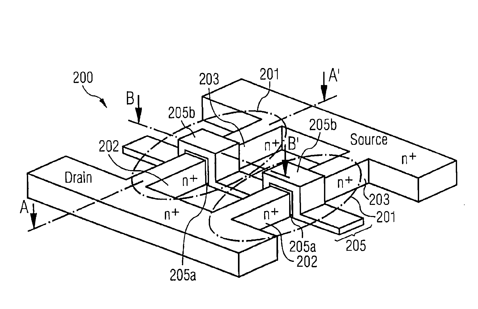
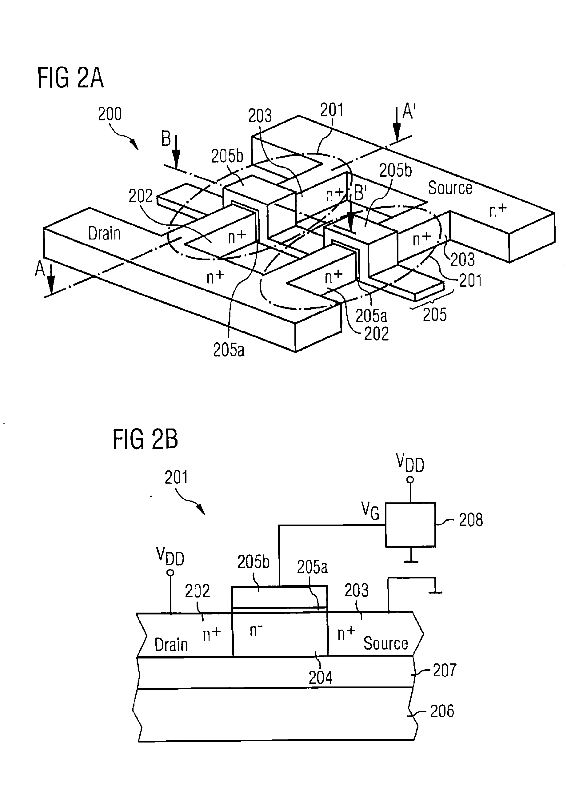
[0099]FIG. 2A shows a device 200 for protection against electrostatic discharges in an electrical circuit with two gate controlled fin resistance elements 201 formed as fin junction field effect transistors (FinJFET) in accordance with one exemplary embodiment of the invention. The gate controlled fin resistance elements 201 have a fin structure, having in each case a heavily n doped (n+ doped) first connection region 202, a heavily n doped (n+ doped) second connection region 203 and also a weakly n doped (n− doped) channel region 204 formed between the first connection region 202 and the second connection region 203, the channel region 204 being concealed by a gate region or gate 205 formed over the side areas and the upper face of the channel region 204, cf. FIG. 2B.

[0100]The fin structures of the gate controlled fin resistance elements 201 have for example a length of between 10 nm and 10 μm, and a width of between 5 nm and 50 nm, and a height of between 5 nm and 200 nm.

[0101]The...


PUM


Abstract

A gate controlled fin resistance element for use as an electrostatic discharge (ESD) protection element in an electrical circuit has a fin structure having a first connection region, a second connection region and a channel region formed between the first and second connection regions. Furthermore, the fin resistance element has a gate region formed at least over a part of the surface of the channel region. The gate region is electrically coupled to a gate control device, which gate control device controls an electrical potential applied to the gate region in such a way that the gate controlled fin resistance element has a high electrical resistance during a first operating state of the electrical circuit and a lower electrical resistance during a second operating state, which is characterized by the occurrence of an ESD event.

Description

CROSS-REFERENCE TO RELATED APPLICATION[0001]This application is claims priority to U.S. patent application Ser. No. 11 / 506,683 filed Aug. 18, 2006, which claims priority to German Patent Application No. DE 10 2005 039 365.9-33 filed Aug. 19, 2005.BACKGROUND[0002]1. Technical Field[0003]The invention relates to a gate controlled fin resistance element for use as electrostatic discharges (ESD) protection element in an electrical circuit, and to a device for protection against electrostatic discharges in an electrical circuit.[0004]2. Description of the Related Art[0005]The development of efficient protection mechanisms for protecting an electronic component against ESD constitutes a growing challenge, particularly when using advanced process technologies such as, for example, MuGFET technologies or FinFET technologies, in view of the ever shrinking dimensions of the electronic devices and the associated increasing sensitivity toward electrical overvoltages.[0006]Electrostatic discharg...

Claims


Application Information

Patent Timeline
Patent Type & Authority Applications(United States)
IPC IPC(8): H02H9/04H01L27/06
CPCH01L27/0288H01L27/1211H01L29/66795H01L29/785H01L29/8086H01L2029/7857H01L29/42392
Inventor GOSSNER, HARALDRUSS, CHRISTIAN
Owner INFINEON TECH AG
Why Eureka
Try Eureka