The dominant ones are high manufacturing costs; difficulty in combining multi-color output from the same
chip; efficiency of light output; and the need for high-cost rigid substrates.
However, in comparison to crystalline-based inorganic LEDs, OLEDs suffer reduced brightness, shorter lifetimes, and require expensive encapsulation for device operation.
Because of problems such as aggregation of the
quantum dots in the emitter layer, the efficiency of these devices was rather low in comparison with typical
OLED devices.
The efficiency was even poorer when a neat film of
quantum dots was used as the emitter layer (Hikmet et al., Journal of Applied
Physics 93, 3509 (2003)).
The poor efficiency was attributed to the insulating nature of the quantum-dot layer.
Regardless of improvements in efficiency, these
hybrid devices still suffer from all of the drawbacks associated with pure
OLED devices.
These organic ligands are insulators and would result in poor
electron and hole injection into the quantum dots.
In addition, the remainder of the structure is costly to manufacture, due to the usage of
electron and hole semiconducting
layers grown by high-vacuum techniques, and the usage of
sapphire substrates.
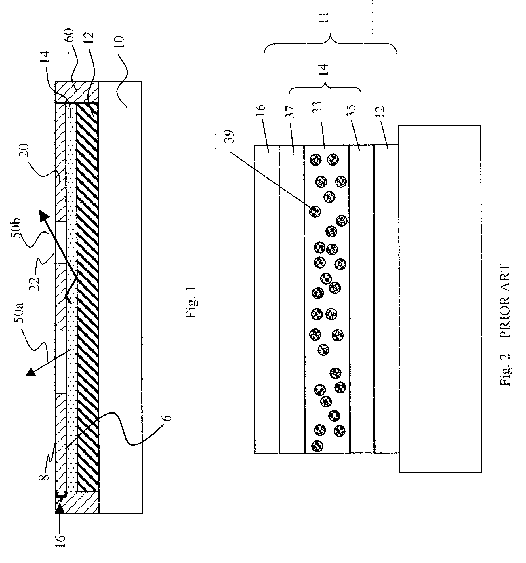
However, the current
carrying capacity of such electrodes is limited, thereby limiting the amount of power that can be supplied to the LED materials, and hence the amount of light that can be emitted from the EL unit.
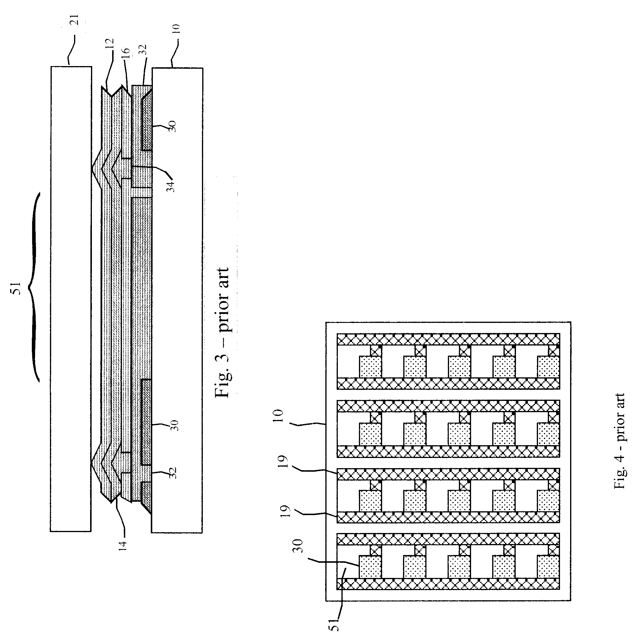
However, the maximum
fill factor is limited by the presence of conductive busses and thin-film electronic components, particularly for bottom-emitting devices.
However, since busses 19 are positioned between light emissive areas 51, the size and
conductivity of busses 19 is limited by the desired
aperture ratio of the emissive area, limiting the amount of current and switching rate of the
OLED device.
Because suitable transparent conductors, for example ITO, have a limited
conductivity, the current that may be passed through the organic layers 14 is limited and the uniformity of the light-emitting areas in an electroluminescent device may be adversely affected by differences in current passed through various portions of the transparent conductor 16.
However, the thick patterned layer of
metal may not be transparent, requiring the
auxiliary electrode 70 to be located between the light-emitting areas, limiting its conductivity and restricting the manufacturing tolerances of the OLED, thereby increasing costs.
Likewise, a typical
black matrix supplied over the OLED device is similarly limited to locations between the light-emitting areas, reducing the contrast of the OLED device.
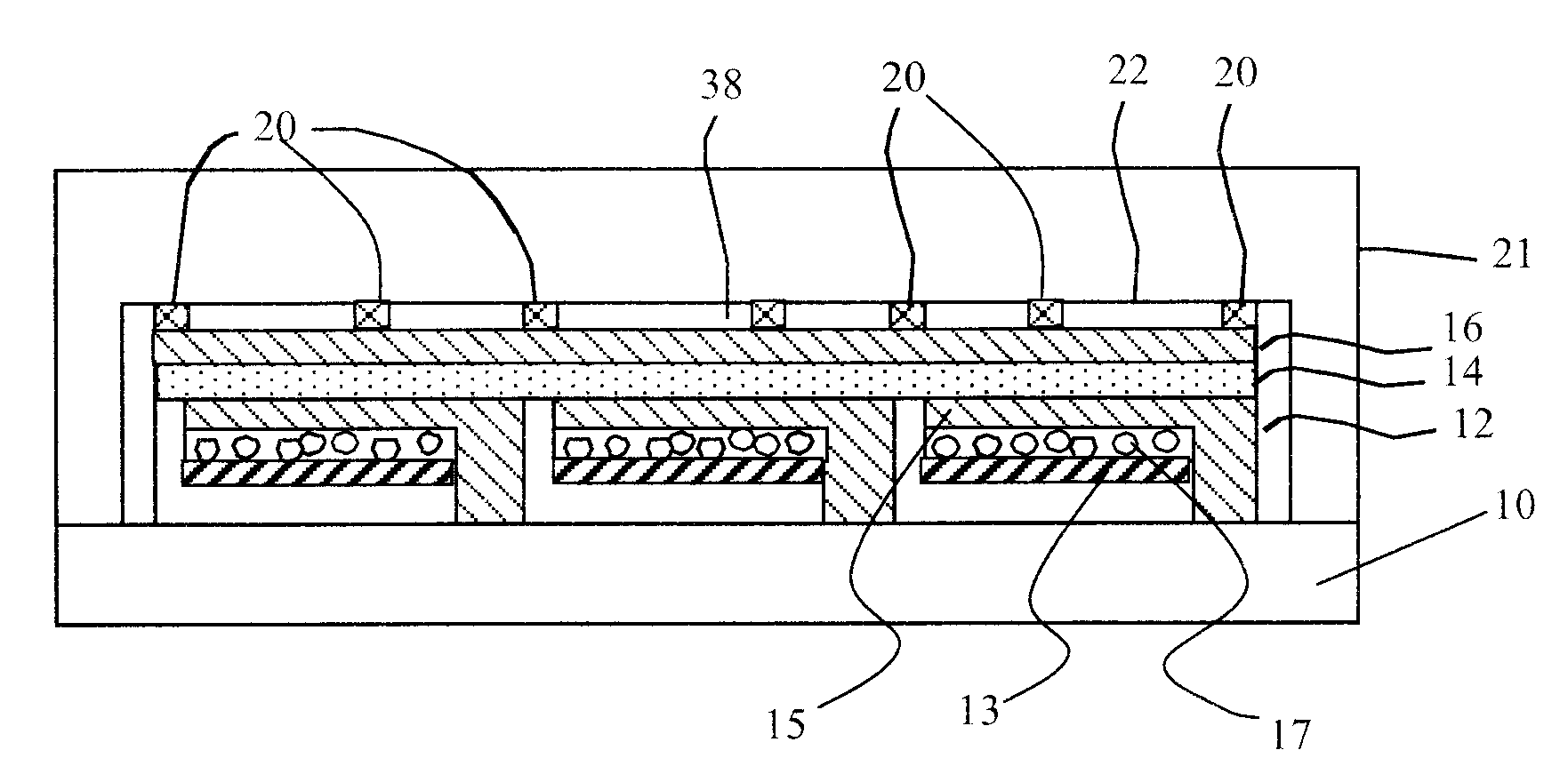
However, for very large devices, the substrate 10 or cover 21, even when composed of rigid materials like glass and employing materials in the gap 38, can bend slightly and cause the inside of the encapsulating cover 21 or materials in the gap 38 to contact or press upon the thin-film layers of materials 12, 14, 16, possibly damaging them and reducing the utility of the OLED device.
Such an application does not, however, provide protection to thin-film layers of materials in an OLED device.
However, in this design, any thin-film layers of materials are not protected when the cover is stressed.
Moreover, the sealing material will reduce the transparency of the device and requires additional manufacturing steps.
However, columnar spacers are formed lithographically and require complex
processing steps and expensive materials.
Moreover, this design is applied to
liquid crystal devices and does not provide protection to thin-film structures deposited on a substrate.
This design does not provide protection to thin-film structures deposited on a substrate.

