

Field-effect semiconductor device
a field-effect semiconductor and semiconductor technology, applied in the field of semiconductor devices, can solve the problems of reducing the electron concentration in reducing the electron concentration of the two-dimensional electron gas layer, and unnecessary complex and expensive associated electric circuitry
- Summary
- Abstract
- Description
- Claims
- Application Information
AI Technical Summary
Benefits of technology
Problems solved by technology
Method used
Image

Examples
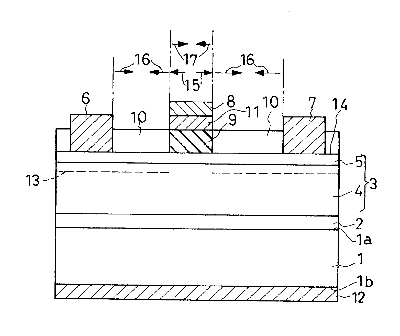
embodiment
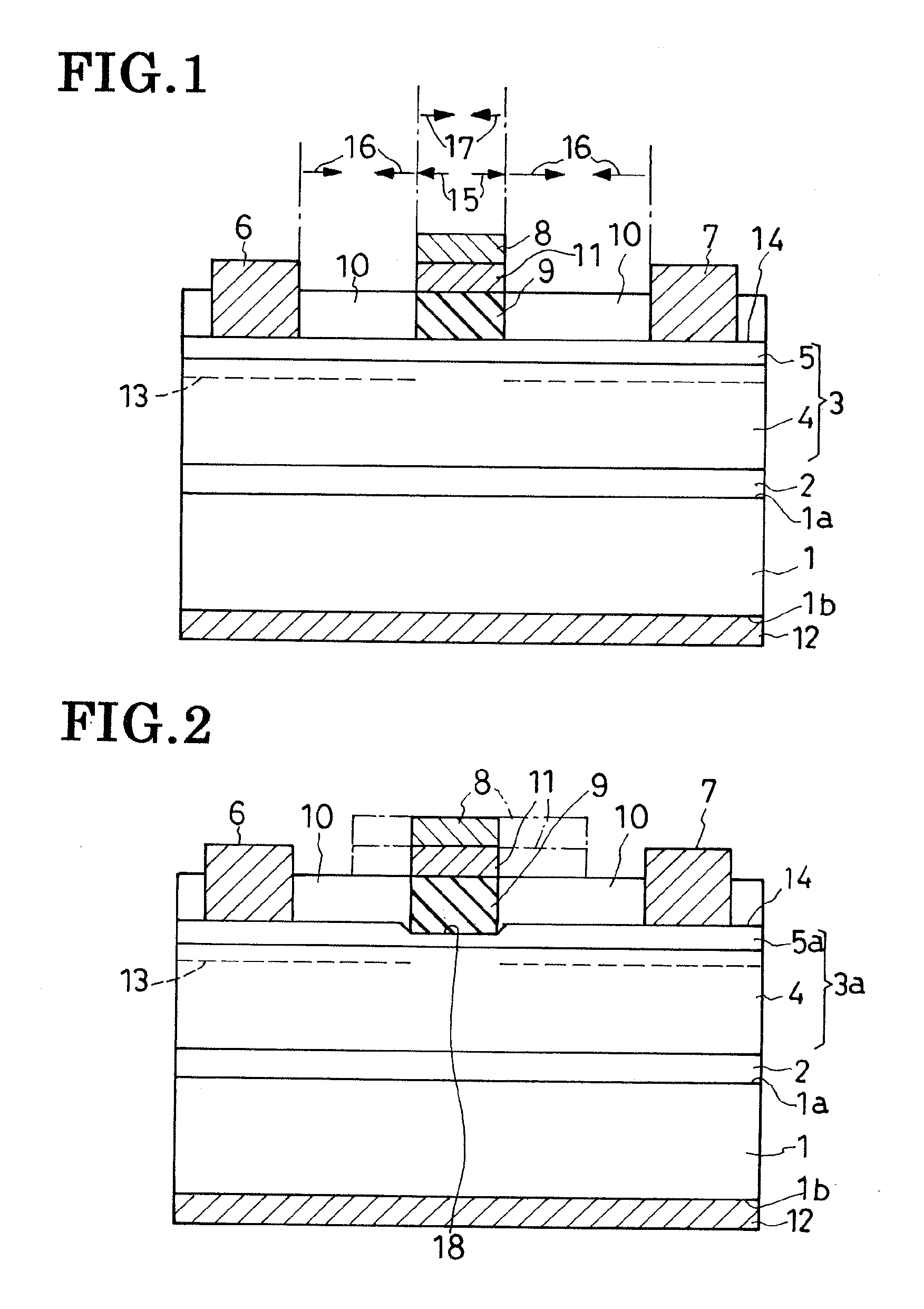
of FIG. 2
[0054]The alternate form of HEMT-type field-effect semiconductor device shown here differs from its FIG. 1 counterpart in having a modified electron supply layer 5a in its main semiconductor region 3a. The electron supply layer 5a has its surface 14 recessed at 18 just under the stack of the gate electrode 8, first insulator 9 and piezoelectric layer 11. The recess 18 is sized to accommodate some lowermost part of the first insulator 9. All the other constructional details of this alternate device are as previously set forth with reference to FIG. 1.
[0055]Let it be assumed that the recessed part of the electron supply layer 5a is as thick as the unrecessed electron supply layer 5 of the first disclosed device. Then, naturally, the other, unrecessed parts of the electron supply layer 5a are thicker than the unrecessed electron supply layer 5. The electric fields due to the piezoelectric and spontaneous depolarizations of these unrecessed parts of the electron supply will the...
PUM
 Abstract
Description
Claims
Application Information