Method for Manufacturing Dielectric Layer Constituting Material, Dielectric Layer Constituting Material Obtained Thereby; Method for Manufacturing Capacitor Circuit Forming Piece Using Dielectric Layer Constituting Material, Capacitor Circuit Forming Piece Obtained Thereby; and Multi-Layer Printed Wiring Board Obtained by Using Dielectric Layer Constituting Material and/or Capacitor Circuit Forming Piece

a technology of dielectric layer and manufacturing method, which is applied in the direction of variable capacitor, fixed capacitor details, etching metal masks, etc., can solve the problems of reduced film thickness uniformity of dielectric layer, increased dielectric loss at transferring signals etc., and achieves the effect of reducing dielectric loss at transferring signals, high quality, and high quality

Active Publication Date: 2008-11-27
MITSUI MINING & SMELTING CO LTD
View PDF6 Cites 18 Cited by
  • Summary
  • Abstract
  • Description
  • Claims
  • Application Information

AI Technical Summary

Benefits of technology

[0034]A multi-layer printed wiring board with an embedded capacitor circuit can be manufactured by popular methods by using a dielectric layer constituting material and / or a capacitor circuit forming piece according to the present invention. Such a multi-layer printed wiring board is a product with an embedded capacitor circuit with high quality.
[0035]The quality of a multi-layer printed wiring board with an embedded capacitor circuit, which is an end product using a dielectric layer constituting material according to the present invention, is dramatically improved because the dielectric layer constituting material obtained by the method for manufacturing a dielectric layer constituting material described above has no unnecessary area of a dielectric layer.
[0036]A method for manufacturing a dielectric layer constituting material and a capacitor circuit forming piece manufactured by using the dielectric layer constituting material according to the present invention is for the purposes of providing a dielectric layer constituting material and a capacitor circuit forming piece that have no dielectric layer in area that do not require the dielectric layer. Manufacturing a multi-layer printed wiring board by using such a dielectric layer constituting material and a capacitor circuit forming piece decreases dielectric loss at transferring signals in a signal circuit close to a capacitor circuit, enables burying other circuit devices such as an inductor, and enables considerably to be free from limiting conditions in circuit design. Therefore, use of a dielectric layer constituting material and a capacitor circuit forming piece obtained by the manufacturing method provides a multi-layer printed wiring board with an embedded capacitor circuit with extremely high quality.

Problems solved by technology

This dielectric layer causes a problem of increasing dielectric loss at transferring signals etc. due to high dielectric constant of the dielectric layer.
Moreover, the dielectric layer usually introduces some restrictions on circuit design because it is often impossible to bury other circuit devices such as an inductor in the dielectric layer.
However, the inventions disclosed in Patent Document 1 (Japanese Patent Laid-Open No. 09-116247), Patent Document (Japanese Patent Laid-Open No. 2000-323845) and Patent Document 3 (Japanese Patent Laid-Open No. 08-125302) almost always cause lack of film thickness uniformity of the dielectric layer, a problem regarding accuracy of position in transferring method and screen printing method, and dielectric strength tests of a capacitor layer has to be conducted for end products, even though the inventions may solve the state remaining of the dielectric layer in unnecessary area.
This is because there is an increasing demand for downsized printed wiring boards in conformity with the particularly recent downsizing trend of electronic and electric equipments, and it is almost impossible to make the area of the capacitor electrode larger in a certain limited area of a printed wiring board.
Therefore, lack of film thickness uniformity cause deviation in quality of capacitors, which is not preferable.
Moreover, problems in accuracy of position in transferring method and screen printing method causes deviation between positions of formed first electrode and second electrode, which decreases effective area of the surface area (A) that determines an electric capacity of a capacitor.
Thus capacitor properties as originally designed cannot be obtained, and product quality becomes out of specification.

Method used


Image

  • Method for Manufacturing Dielectric Layer Constituting Material, Dielectric Layer Constituting Material Obtained Thereby; Method for Manufacturing Capacitor Circuit Forming Piece Using Dielectric Layer Constituting Material, Capacitor Circuit Forming Piece Obtained Thereby; and Multi-Layer Printed Wiring Board Obtained by Using Dielectric Layer Constituting Material and/or Capacitor Circuit Forming Piece
  • Method for Manufacturing Dielectric Layer Constituting Material, Dielectric Layer Constituting Material Obtained Thereby; Method for Manufacturing Capacitor Circuit Forming Piece Using Dielectric Layer Constituting Material, Capacitor Circuit Forming Piece Obtained Thereby; and Multi-Layer Printed Wiring Board Obtained by Using Dielectric Layer Constituting Material and/or Capacitor Circuit Forming Piece
  • Method for Manufacturing Dielectric Layer Constituting Material, Dielectric Layer Constituting Material Obtained Thereby; Method for Manufacturing Capacitor Circuit Forming Piece Using Dielectric Layer Constituting Material, Capacitor Circuit Forming Piece Obtained Thereby; and Multi-Layer Printed Wiring Board Obtained by Using Dielectric Layer Constituting Material and/or Capacitor Circuit Forming Piece

Examples


example 1

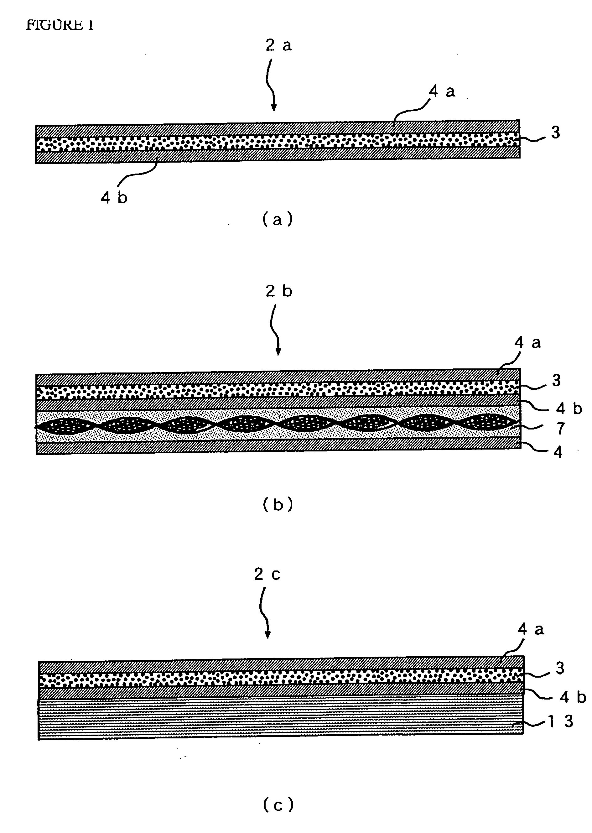
Manufacturing a Dielectric Layer Constituting Material

[0125]Step a (a step for forming a first electrode circuit): At the beginning, a binder resin solution was prepared. In the preparation of the binder resin solution, the raw materials used were 25 parts by weight of phenol novolac type epoxy resin, 25 parts by weight of a solvent soluble aromatic polyamide resin polymer BP3225-50P commercially available as a blended varnish mixed with cyclopentanone as solvent from Nippon Kayaku Co., Ltd. To finish preparation of a resin mixture having the blending ratios shown below, curing agent MEH-7500a, novolac type phenolic resin from Meiwa Plastic Industries, Ltd., and a curing accelerator 2E4MZ from SHIKOKU CHEMICALS CORPORATION were added to the varnish.

[0126]The composition of the binder resin:

Phenol novolac type epoxy resin 39 parts by weightAromatic polyamide resin polymer 39 parts by weightNovolac type phenolic resin 22 parts by weightCuring accelerator0.1 parts by weight

[0127]The re...

example 2

[0136]A manufacturing method used in Example 2 is basically the same as Example 1 except the method for removing the dielectric layer. Therefore, description regarding processes to be redundant explanation is omitted, and only the method for removing the dielectric layer will be explained.

[0137]In this Example, the dielectric layer was removed by a de-smear treatment. Unnecessary dielectric layer was dissolved and removed with a commercially available de-smear solution.

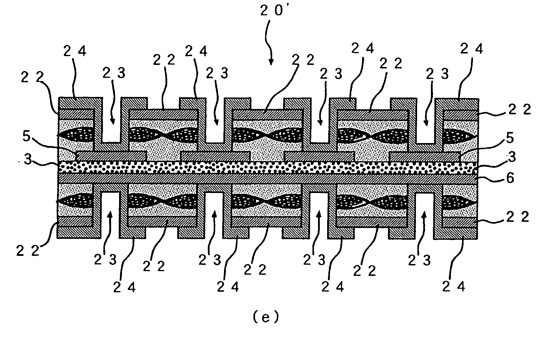
[0138]In the procedure mentioned above, a multi-layer printed wiring board 20 comprising an embedded capacitor circuit was manufactured. As a result, an extremely excellent multi-layer printed wiring board was obtained.

example 3

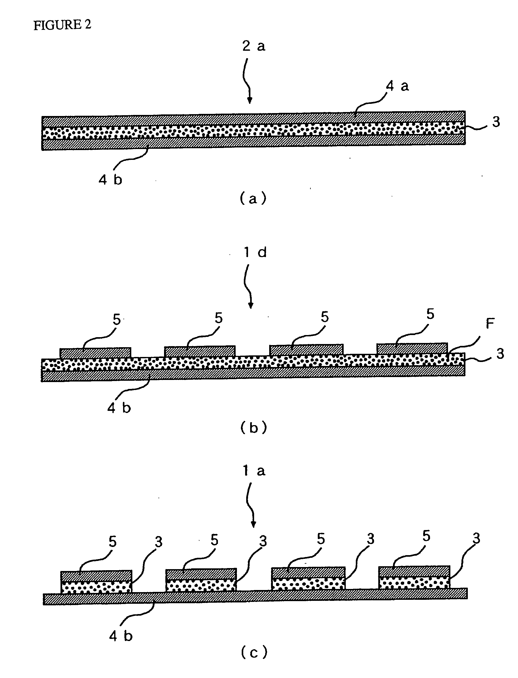
Manufacturing a Capacitor Circuit Forming Piece with a Carrier Layer

[0139]As mentioned above, a copper foil with a carrier foil was used as the second conductor layer. The copper foil with a carrier foil comprises a peelable type and an etchable type, and either of which may be used. But the peelable type is preferably used because processes can be simplified. Among the peelable type used was the type which used no heavy metal on a bonding interface and had an organic bonding interface between the carrier foil and the conductor layer using triazole compounds having substituents such as 1,2,3-benzotriazole or carboxybenzotriazole.

[0140]A dry film was laminated to the surface of the first conductor layer (electrode circuit) of the dielectric layer constituting material in FIG. 13(a) that underwent the step a and the step b in which a dielectric layer was removed; and etching patterns were exposed and developed to obtain what is shown in FIG. 13(b). Then the first conductor layer was e...


PUM

PropertyMeasurementUnit
particle sizeaaaaaaaaaa
thickaaaaaaaaaa
pressureaaaaaaaaaa

Abstract

An object is to obtain a dielectric layer constituting material, a capacitor circuit forming piece, etc. in which unnecessary dielectric layer is removed except capacitor circuit parts that improve accuracy of position of an embedded capacitor circuit in a multi-layer printed wiring board. For the purpose of achieving the object, “a method for manufacturing a dielectric layer constituting material characterized in that step a is a step for forming a first electrode circuit by etching a conductor layer on one side of a metal clad dielectric comprising a conductor layer on each side of a dielectric layer; step b is a step for removing the dielectric layer that is exposed between the first electrode circuits to manufacture the dielectric layer constituting material; and the step a is conducted and then the step b is conducted” is adopted. Then as a process for manufacturing a capacitor circuit forming piece, the dielectric layer constituting material obtained above is used and a process for forming a second electrode at a position facing the first electrode is conducted.

Description

TECHNICAL FIELD[0001]The present invention provides a method for manufacturing a dielectric layer constituting material, a dielectric layer constituting material obtained by the method; a method for manufacturing a capacitor circuit forming piece by using the dielectric layer constituting material, a capacitor circuit forming piece obtained by the method; and a multi-layer printed wiring board with an embedded capacitor circuit manufactured by using the dielectric layer constituting material and / or the capacitor circuit forming piece.BACKGROUND ART[0002]Conventionally, a multi-layer printed wiring board with an embedded capacitor circuit uses one or more insulating layer(s) locating in the inner layer of the board as dielectric layer(s). An inner layer circuit locating on each side of the dielectric layer includes a capacitor: a first electrode circuit and a second electrode circuit, which face each other. Therefore, such a capacitor circuit is sometimes referred to as an embedded c...

Claims


Application Information

Patent Timeline
Patent Type & Authority Applications(United States)
IPC IPC(8): H01G4/06H05K1/16
CPCH05K1/0366Y10T29/49155H05K3/002H05K3/0044H05K3/20H05K3/4614H05K3/4652H05K2201/0209H05K2201/09509H05K2203/025H05K2203/0554Y10T29/435Y10T29/49156Y10T29/43Y10T29/49128H05K1/162H05K3/46
Inventor NAKAMURA, KENSUKEYAMAZAKI, KAZUHIRO
Owner MITSUI MINING & SMELTING CO LTD
Why Eureka
Try Eureka