Method of forming amorphous carbon film and method of manufacturing semiconductor device using the same
Inactive Publication Date: 2008-11-27
TES CO LTD
View PDF7 Cites 183 Cited by
Summary
Abstract
Description
Claims
Application Information
AI Technical Summary
This helps you quickly interpret patents by identifying the three key elements:
Problems solved by technology
Method used
Benefits of technology
Benefits of technology
[0010]The present invention provides a method of forming an amorphous carbon film capable of forming desired patterns without the occurrence of diffused reflection by forming an amorphous carbon film whose refractive index can be finely controllable and light absorption coefficient is low.
[0011]Further, the present invention provides a method of forming an amorphous carbon film where a small amount of reaction by-products is generated, a chamber is hardly contaminated, the reaction by-products are easily removed and thus cost and processing time can be saved.
[0012]Furthermore, the present invention provides a method of manufacturing a semiconductor device using an amorphous carbon film, wherein the amorphous carbon film is formed by vaporizing a liquid hydrocarbon compound, and a photosensitive film can be accurately patterned without an anti-reflection film by using the amorphous carbon film as a hard mask film.
Problems solved by technology
However, when the thickness of the photosensitive film pattern is undesirably thin, the photosensitive film pattern can be etched away ahead of the lower material layer that is thicker than the photosensitive film pattern, whereby a lower material layer pattern can not be formed.
When the linewidth is small, however, the photosensitive film pattern collapses during the etching process of the hard mask.
Accordingly, it is not possible to pattern the hard mask film and the lower material layer.
Further, if the thickness of the hard mask film is increased, productivity of the apparatus per unit time is decreased.
Productivity decrease in the subsequent etching process and troubles caused by impurities become more probable as well.
As a result, necking and footing occur in the developing process due to the diffused reflection.
Further, the reduction of the cross-sectional area increases the resistance of the wire, lowers down the processing speed of the device and damages the reliability of the device by facilitating movement of electrons.
When using the above-mentioned materials, however, it is not possible to freely adjust a deposition rate, an etching selectivity, a refractive index (n), a light absorption coefficient (k), and stress characteristics.
Because the reaction by-products are usually stuck to the inner wall of a chamber, a cleaning process should be performed more often, which result in a longer processing time and a higher cost.
Meanwhile, the reaction by-products are not easily removed from the chamber in the cleaning process.
As a result, the quality of the amorphous carbon film deteriorates and parts changing cycles of a chamber are shortened.
Method used
Image
Click on the blue label to locate the original text in one second.
Reading with bidirectional positioning of images and text.
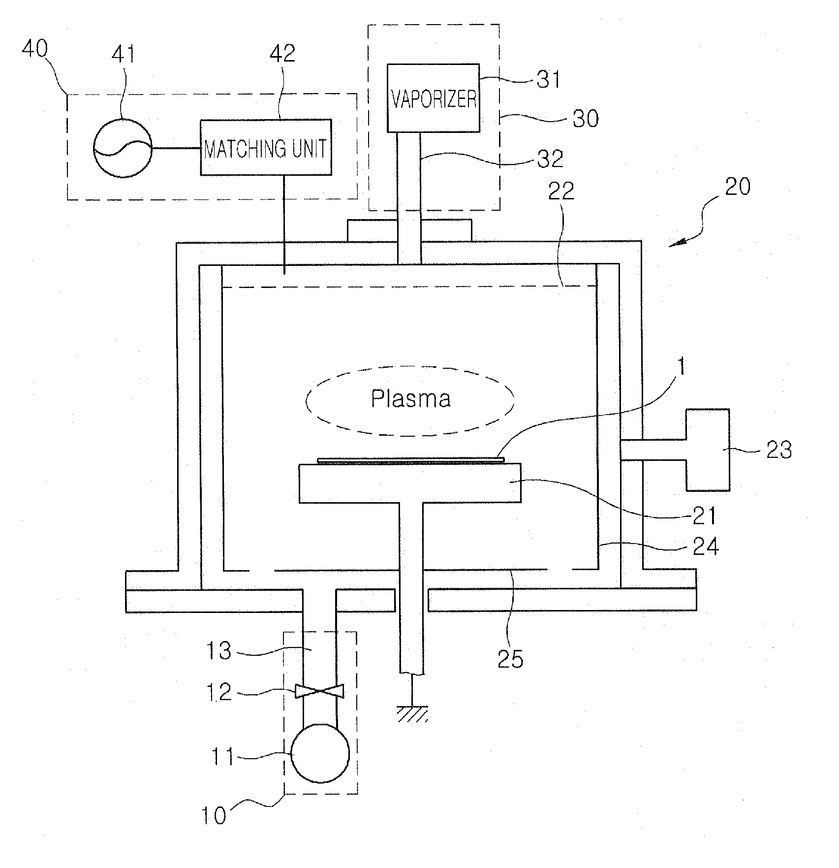
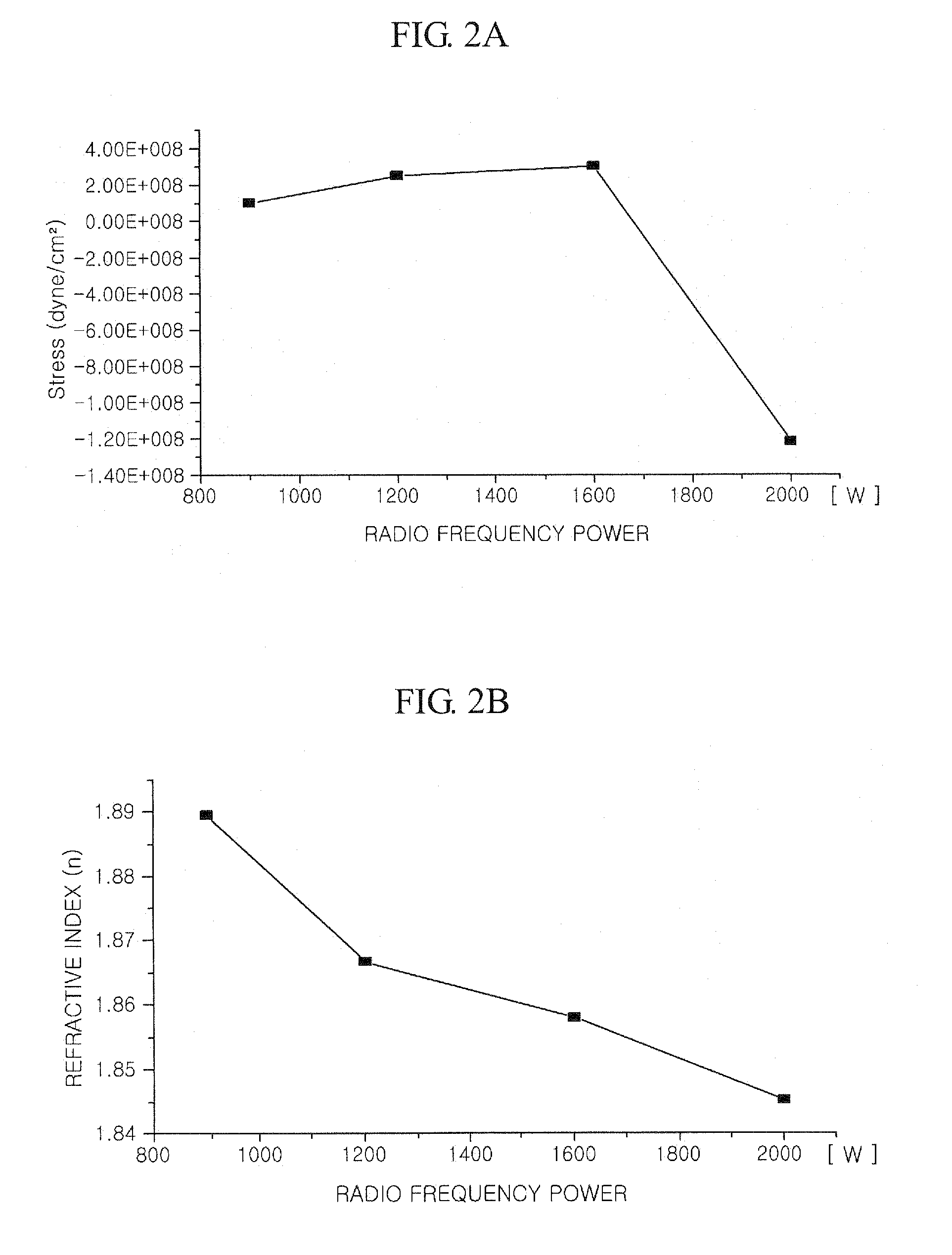
[0057]In a first example of the present invention, an amorphous carbon film was formed by supplying hexene (C6H12) at a flow rate of 0.8 g / min, argon at a flow rate of 300 sccm, and helium at a flow rate of 800 sccm at a pressure of 7 Torr and temperature of 550° C. while radio frequency power is changed in a range of 900 to 2000 W. Further, a distance of 350 mils was maintained between the shower head and the substrate. FIGS. 2A to 2D illustrate changes in stress, refractive index (n), light absorption coefficient (k), and deposition rate of the amorphous carbon film, depending on radio frequency power, respectively.
[0058]FIG. 2A is a graph illustrating a change in stress of the amorphous carbon film depending on radio frequency power. Referring to FIG. 2A, as radio frequency power increases, stress slightly increases and then significantly decreases after the radio frequency power becomes 1600 ...
second example
Change in Characteristics of an Amorphous Carbon Film Depending on the Amount of Reaction Source to be Supplied
[0064]In a second example of the present invention, an amorphous carbon film was formed by supplying hexene (C6H12) at a flow rate in the range of 0.3 to 0.8 g / min, argon at a flow rate of 300 sccm, and helium at a flow rate of 200 sccm at a pressure of 7 Torr and temperature of 550° C. while the radio frequency power of 1600 W is applied. Further, a distance of 320 mils was maintained between the shower head and the substrate. In this case, FIGS. 3A to 3D illustrate changes in stress, refractive index (n), light absorption coefficient (k), and deposition rate of the amorphous carbon film, depending on the amount of reaction source to be supplied, respectively.
[0065]FIG. 3A is a graph illustrating a change in stress of the amorphous carbon film depending on the amount of reaction source to be supplied. Referring to FIG. 3A, as the amount of reaction source to be supplied in...
third example
Change in Characteristics of an Amorphous Carbon Film Depending on a Distance Between the Shower Head and the Substrate
[0071]In a third example of the present invention, an amorphous carbon film was formed by supplying hexene (C6H12) at a flow rate of 0.8 g / min, argon at a flow rate of 300 sccm, and helium at a flow rate of 800 sccm at a pressure of 7 Torr and temperature of 550° C. while radio frequency power of 1600 W is applied. Further, a distance between the shower head and the substrate was changed in the range of 250 to 350 mils. In this case, FIGS. 4A to 4D illustrate changes in stress, refractive index (n), light absorption coefficient (k), and deposition rate of the amorphous carbon film, depending on a distance between the shower head and the substrate, respectively.
[0072]FIG. 4A is a graph illustrating a change in stress of the amorphous carbon film depending on a distance between the shower head and the substrate. Referring to FIG. 3A, as the distance between the shower...
PUM
Property
Measurement
Unit
Temperature
aaaaa
aaaaa
Pressure
aaaaa
aaaaa
Power
aaaaa
aaaaa
Abstract
The present invention relates to a method of forming an amorphous carbon film and a method of manufacturing a semiconductor device using the method. An amorphous carbon film is formed on a substrate by vaporizing a liquid hydrocarbon compound, which has chain structure and one double bond, and supplying the compound to a chamber, and ionizing the compound. The amorphous carbon film is used as a hard mask film.It is possible to easily control characteristics of the amorphous carbon film, such as a deposition rate, an etching selectivity, a refractive index (n), a light absorption coefficient (k) and stress, so as to satisfy user's requirements. In particular, it is possible to lower the refractive index (n) and the light absorption coefficient (k). As a result, it is possible to perform a photolithography process without an antireflection film that prevents the diffuse reflection of a lower material layer.Further, a small amount of reaction by-product is generated during a deposition process, and it is possible to easily remove reaction by-products that are attached on the inner wall of a chamber. For this reason, it is possible to increase a cycle of a process for cleaning a chamber, and to increase parts changing cycles of a chamber. As a result, it is possible to save time and cost.
Description
BACKGROUND OF THE INVENTION[0001]1. Field of the Invention[0002]The present invention relates to a method of forming an amorphous carbon film, and more particularly, to a method of forming an amorphous carbon film having a low light absorption coefficient and a wide range of refractive index by using a liquid hydrocarbon compound, and a method of manufacturing a semiconductor device using the method.[0003]2. Description of the Related Art[0004]A semiconductor device includes various elements such as word lines, bit lines, capacitors, and metal wires, which interact with one another. As a degree of integration and a performance of a semiconductor device increase, demand for materials and process technologies for manufacturing the semiconductor device is also increasing. In particular, the increase of the degree of integration is accompanied with a decrease of the size of a semiconductor device, a method of forming fine patterns for various structures on a semiconductor substrate has ...
Claims
Application Information
Patent Timeline
Application Date:The date an application was filed.
Publication Date:The date a patent or application was officially published.
First Publication Date:The earliest publication date of a patent with the same application number.
Issue Date:Publication date of the patent grant document.
PCT Entry Date:The Entry date of PCT National Phase.
Estimated Expiry Date:The statutory expiry date of a patent right according to the Patent Law, and it is the longest term of protection that the patent right can achieve without the termination of the patent right due to other reasons(Term extension factor has been taken into account ).
Invalid Date:Actual expiry date is based on effective date or publication date of legal transaction data of invalid patent.

