Method for processing a semiconductor device comprising a silicon-oxy-nitride dielectric layer

a technology of siliconoxynitride and dielectric layer, which is applied in the direction of semiconductor devices, basic electric elements, electrical apparatus, etc., can solve the problems of gate leakage, unacceptable increase of gate tunneling current, and significant limitation of cmos downscaling effect, so as to reduce gate leakage current and be well controlled

Active Publication Date: 2005-06-16
NXP BV +1
View PDF2 Cites 0 Cited by
  • Summary
  • Abstract
  • Description
  • Claims
  • Application Information

AI Technical Summary

Benefits of technology

[0005] It is an object of the present invention to avoid the above drawbacks and to provide a method for processing a semiconductor device comprising a silicon-oxy-nitride dielectric layer that is very thin and that reduces the gate leakage current in the device, wherein the method is simple and well controllable.
[0009] In an aspect of the first embodiment, providing a silicon oxide control electrode dielectric layer comprises providing a silicon oxide control electrode dielectric layer with an atomic silicon to oxygen ratio substantially equal to ½ and subsequently incorporating additional silicon atoms into the formed silicon oxide control electrode dielectric layer, e.g., by implantation. This step is particularly suitable for use with a thermal silicon oxide, in that it provides the highest quality both with respect to the interface with silicon as well as with respect to defect density. It is also very easy to form. The silicon atoms can be incorporated into the silicon dioxide layer by either ion implantation or by plasma implantation.
[0011] The silicon oxide dielectric layer can be provided by a deposition technique such as, for example, chemical vapor deposition (CVD), which is generally preferred as it is more suitable for the large-scale production of MOS ICs. Other suitable deposition techniques include sputtering, plasma enhanced CVD (PECVD), and atomic layer deposition (ALD). In this way, it is very simple to introduce a stepwise or gradual profile in the atomic silicon to oxygen ratio in the dielectric layer.
[0016] An advantage of the methods of the preferred embodiments is that it becomes possible to form very thin dielectric layers, through which gate leakage can be reduced or suppressed.
[0017] Semiconductor devices according to the preferred embodiments offer the important advantage of a well controlled and very thin dielectric layer, e.g., of less than 1.5 nm, the latter being required for sub 100 nm CMOS technology, and a high quality interface between dielectric region and semiconductor substrate, e.g., silicon semiconductor substrate.

Problems solved by technology

However, reducing the SiO2 thickness below 3 nm has resulted in such deleterious effects as penetration of dopant atoms of the polysilicon gate, such as, for example, boron, and hence an unacceptable increase in gate tunneling current (gate leakage).
This effect has become a significant limitation in CMOS downscaling as this is paired with an increasingly thin dielectric region being required.
A drawback of the method described above is that the beneficial effect of the incorporation of nitrogen into the dielectric layer is still not satisfactory for very thin dielectric layers.
Gate leakage may still occur in such cases.
This drawback grows in importance as dielectric layers become thinner.

Method used


Image

  • Method for processing a semiconductor device comprising a silicon-oxy-nitride dielectric layer
  • Method for processing a semiconductor device comprising a silicon-oxy-nitride dielectric layer
  • Method for processing a semiconductor device comprising a silicon-oxy-nitride dielectric layer

Examples


Embodiment Construction

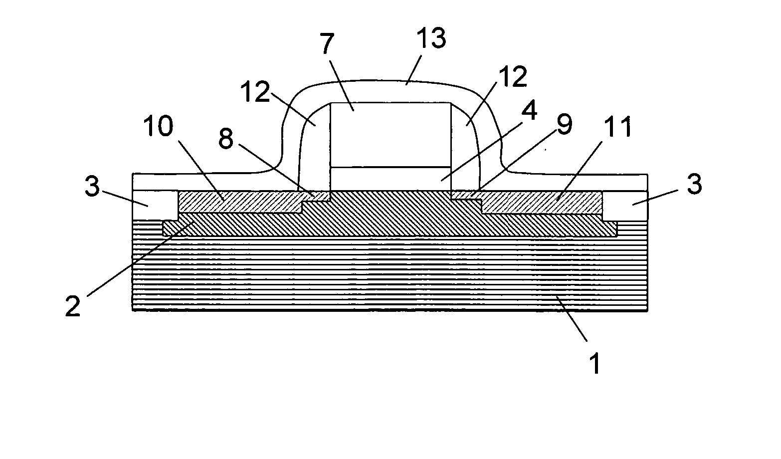
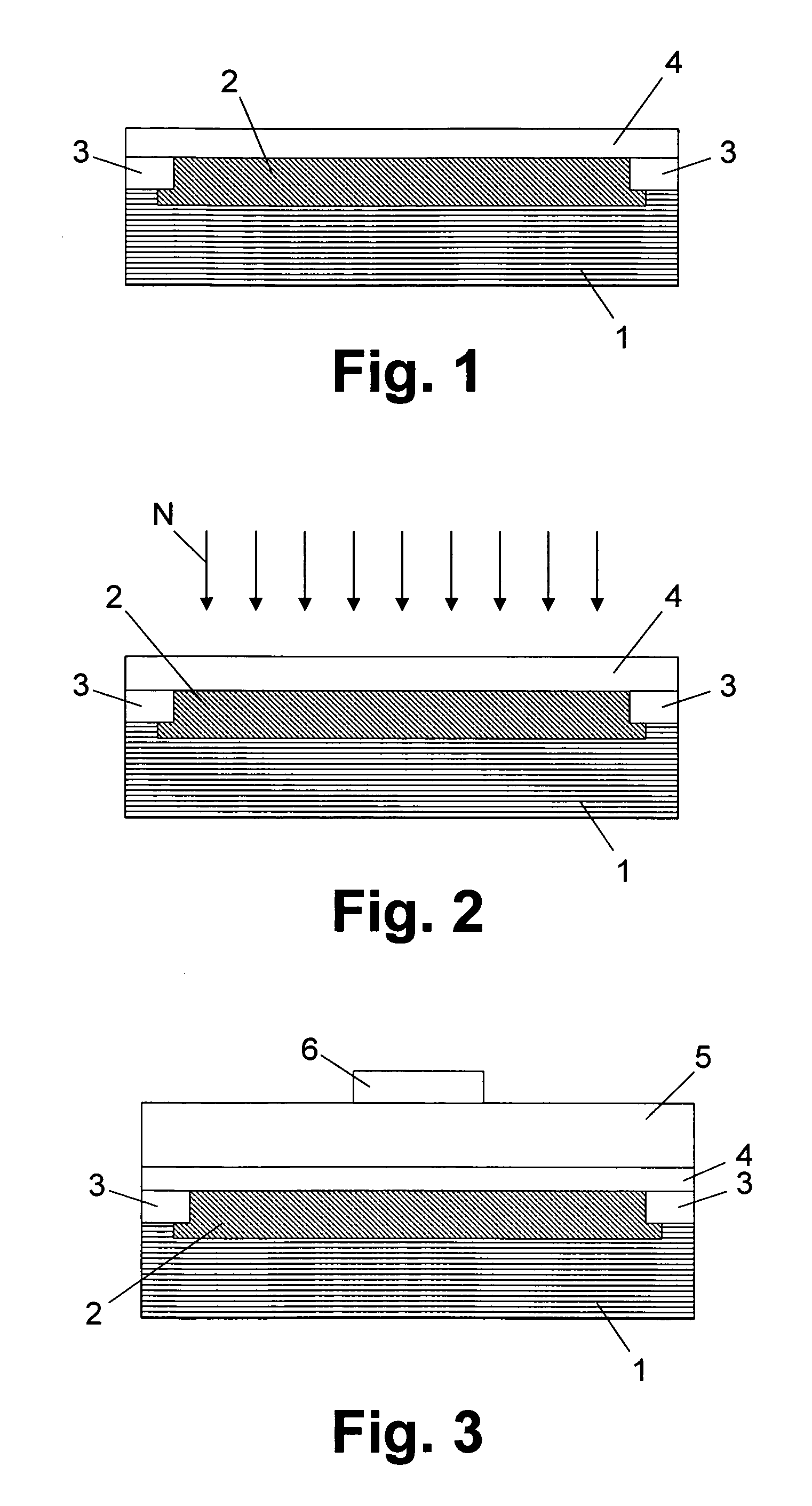
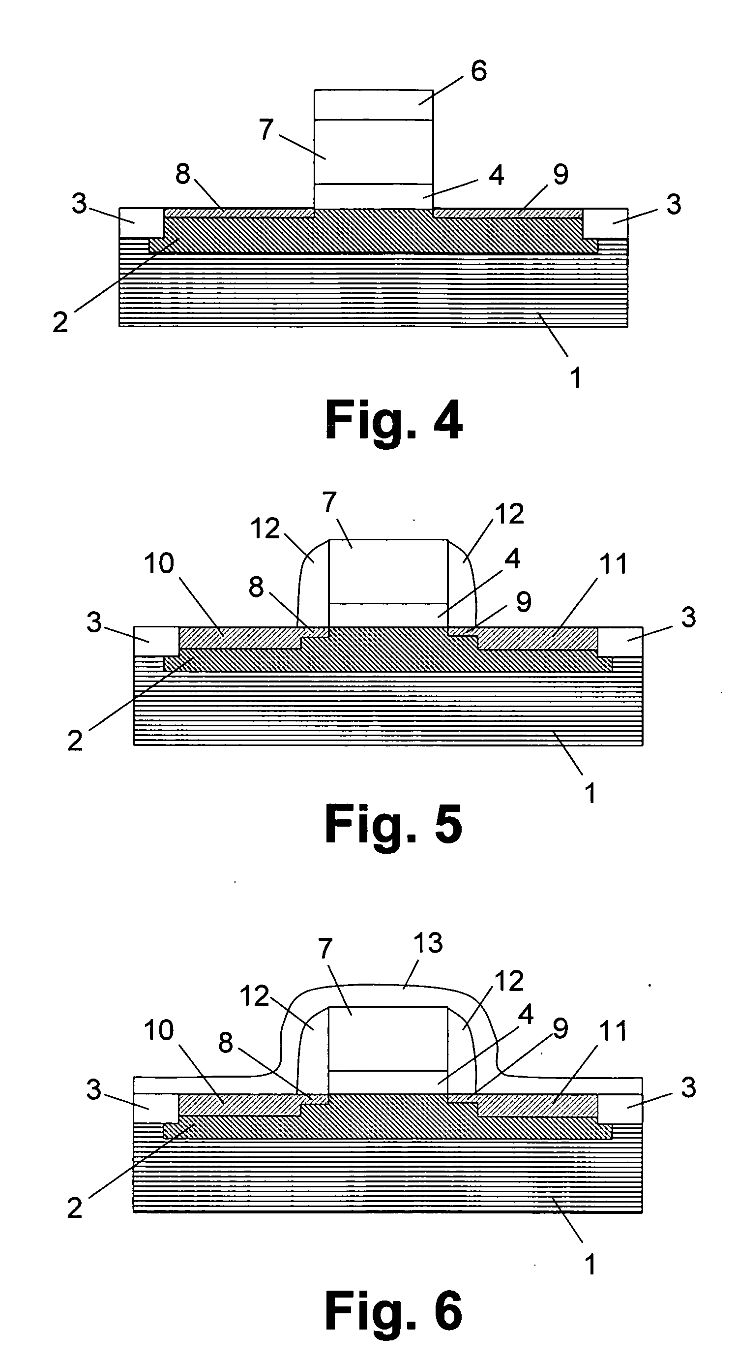
[0033] The following description and examples illustrate a preferred embodiment of the present invention in detail. Those of skill in the art will recognize that there are numerous variations and modifications of this invention that are encompassed by its scope. Accordingly, the description of a preferred embodiment should not be deemed to limit the scope of the present invention.

[0034] The drawings described are only schematic and are non-limiting. In the drawings, the size of some of the elements may be exaggerated and not drawn on scale for illustrative purposes. In particular, the dimensions in the thickness direction are exaggerated for greater clarity.

[0035] Furthermore, the terms first, second, third, and the like in the description and in the claims are used for distinguishing between similar elements and not necessarily for describing a sequential or chronological order. It is to be understood that the terms so used are interchangeable under appropriate circumstances and ...


PUM

PropertyMeasurementUnit
thicknessaaaaaaaaaa
thicknessaaaaaaaaaa
thicknessaaaaaaaaaa

Abstract

The present invention provides a method for processing a semiconductor device wherein a dielectric layer is partially converted into a silicon-oxy-nitride by incorporation of nitrogen atoms into the dielectric layer, which comprises a silicon oxide. Before the introduction of the nitrogen atoms into the dielectric layer, the dielectric layer is provided as a silicon oxide in which the atomic silicon to oxygen ration is greater than ½. In this way, MOS transistors are obtained with a high quality interface between the dielectric region and semiconductor substrate, and a dielectric region which is impermeable to impurity atoms from the gate region and which has a thickness which is substantially equal to the dielectric layer as deposited.

Description

FIELD OF THE INVENTION [0001] The present invention relates to a semiconductor device comprising an insulating layer of silicon-oxy-nitride material, and to a method of manufacturing such a semiconductor device. BACKGROUND OF THE INVENTION [0002] Gate dielectric thickness in, for example, CMOS technology is continually scaled down with each technology node. For instance, sub 100 nm CMOS (Complementary MOS) technology requires a gate dielectric, assuming a doped silicon dioxide (SiO2) layer with a layer thickness below 1.5 nm. However, reducing the SiO2 thickness below 3 nm has resulted in such deleterious effects as penetration of dopant atoms of the polysilicon gate, such as, for example, boron, and hence an unacceptable increase in gate tunneling current (gate leakage). This effect has become a significant limitation in CMOS downscaling as this is paired with an increasingly thin dielectric region being required. The addition of nitrogen (N) to the dielectric layer in order to for...

Claims


Application Information

Patent Timeline
Patent Type & Authority Applications(United States)
IPC IPC(8): H01L21/265H01L21/28H01L21/318H01L29/51H01L29/78
CPCH01L21/265H01L21/28194H01L29/518H01L29/513H01L21/28202
Inventor VENEZIA, VINCENT CHARLESCUBAYNES, FLORENCE NATHALIE
Owner NXP BV
Why Eureka
Try Eureka