Method for Fabricating a Nanoelement Field Effect Transistor with Surrounded Gate Structure

a technology of element field and transistor, which is applied in the manufacture of nanostructures, semiconductor devices, electrical devices, etc., can solve the problems of increasing the waste heat, developing ever smaller and densely arranged transistors, and subject to fundamental physical problems and restrictions, and achieves the effect of successfully controlling

Inactive Publication Date: 2008-12-04
POLARIS INNOVATIONS LTD
View PDF7 Cites 19 Cited by
  • Summary
  • Abstract
  • Description
  • Claims
  • Application Information

AI Technical Summary

Benefits of technology

[0016]One basic idea of the invention is that of removing a surface region of a substrate after the formation of a planar nanoelement, in such a manner that a region of the nanoelement is uncovered over its entire periphery. This uncovered region is covered over its entire periphery with a gate-insulating structure, and the latter is in turn covered over its entire periphery with a gate structure, thereby creating a gate region that surrounds the entire periphery of the nanoelement. This allows particularly sensitive control of the electrical conductivity of the channel region of the nanoelement field effect transistor, which channel region is formed by the nanoelement region between the two end portions coupled to the source / drain regions.
[0027]The removed surface region of the substrate can be completely or partially filled with the gate-insulating structure and with the gate structure. According to this configuration, material-free regions, which may be mechanically unstable, in the semiconductor technology product obtained are reduced or avoided, resulting in a good quality being achieved.

Problems solved by technology

In particular, the development of ever smaller and densely arranged transistors, nowadays amounting to several hundred millions of transistors per chip, will be subject to fundamental physical problems and restrictions within the next ten years.
The increase in integration density of components on a chip also leads to a dramatic increase in the waste heat.
One problem with integrated circuit components based on nanoelements according to the prior art is that the controlled formation and driving of nanoelement components of this type is difficult.

Method used


Image

  • Method for Fabricating a Nanoelement Field Effect Transistor with Surrounded Gate Structure
  • Method for Fabricating a Nanoelement Field Effect Transistor with Surrounded Gate Structure
  • Method for Fabricating a Nanoelement Field Effect Transistor with Surrounded Gate Structure

Examples


Embodiment Construction

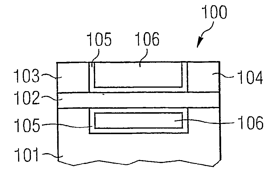
[0074]The text that follows, referring to FIG. 1, provides a description of a carbon nanotube field effect transistor 100 in accordance with a preferred exemplary embodiment of the invention.

[0075]The carbon nanotube field effect transistor 100 has a silicon oxide substrate 101 and a carbon nanotube 102 formed on the silicon oxide substrate 101. A first end portion of the carbon nanotube 102 is formed with a first source / drain region 103 of metallic material, such as for example palladium, titanium, gold, cobalt, tantalum, tungsten or molybdenum, on the silicon oxide substrate 101. Furthermore, a second source / drain region 104 of metallic material, such as for example palladium, titanium, gold, cobalt, tantalum, tungsten or molybdenum, is formed on the silicon oxide substrate 101, which second source / drain region 104 is coupled to a second end portion of the carbon nanotube 102. A removed surface region of the silicon oxide substrate 101, which has been removed below a central porti...


PUM


Abstract

A nanoelement field effect transistor includes a nanotube disposed on the substrate. A first source / drain region is coupled to a first end portion of the nanoelement and a second source / drain region is coupled to a second end portion of the nanoelement. A recess in a surface region of the substrate is arranged in such a manner that a region of the nanoelement arranged between the first and second end portions is taken out over the entire periphery of the nanoelement. A gate-insulating structure covers the periphery of the nanoelement and a gate structure covers the periphery of the gate-insulating structure.

Description

[0001]This is a divisional application of U.S. application Ser. No. 11 / 482,493, which was filed on Jul. 7, 2006, which is a continuation of co-pending International Application No. PCT / DE2005 / 0000001, filed Jan. 3, 2005, which designated the United States and was not published in English, and which is based on German Application No. 10 2004 001 340.3 filed Jan. 8, 2004, all of which applications are incorporated herein by reference.TECHNICAL FIELD[0002]The invention relates to a method for fabricating a nanoelement field effect transistor, to a nanoelement field effect transistor and to a nanoelement array.BACKGROUND[0003]As miniaturization progresses, conventional silicon microelectronics will reach its limits. In particular, the development of ever smaller and densely arranged transistors, nowadays amounting to several hundred millions of transistors per chip, will be subject to fundamental physical problems and restrictions within the next ten years. When feature sizes drop below...

Claims


Application Information

Patent Timeline
Patent Type & Authority Applications(United States)
IPC IPC(8): H01L29/12B82B3/00H01L21/336H01L29/06H01L29/78H01L51/05H01L51/30H01L51/40
CPCB82Y10/00H01L29/0665H01L29/0673H01L51/0048H01L51/0545Y10S977/813Y10S977/72Y10S977/742Y10S977/762H10K85/221H10K10/466
Inventor KREUPL, FRANZSEIDEL, ROBERT
Owner POLARIS INNOVATIONS LTD
Why Eureka
Try Eureka