Organic Silane Compound, Method of Producing the Same, and Organic Thin Film Using the Same

a technology of organic silane and compound, which is applied in the direction of organic chemistry, non-metal conductors, organic conductors, etc., can solve the problems of difficult formation of thin films in the solution process, and achieve the effects of high stabilized, effective physical exfoliation, and high crystallization

Inactive Publication Date: 2008-12-18
SHARP KK
View PDF14 Cites 2 Cited by
  • Summary
  • Abstract
  • Description
  • Claims
  • Application Information

AI Technical Summary

Benefits of technology

[0014]The organic silane compound according to the invention, which has a terminal silyl group, forms a network of silicon and oxygen atoms among neighboring compound molecules and binds to the substrate chemically via a silanol bond, for example, when an organic thin film is formed. As a result, the organic thin film is very highly stabilized and highly crystallized. Thus, the thin film obtained is adsorbed on the base material surface more tightly than the film physically adsorbed on the base material, preventing physical exfoliation effectively.
[0015]In addition, the organic silane compound according to the invention has a fused polycyclic aromatic hydrocarbon skeleton that is π-electron conjugated; high π-electron interaction and intermolecular interaction (van der Waals interaction) are generated among neighboring molecules in an organic thin film; and thus, the resulting film obtained is superior in semiconductor characteristics and higher in crystallinity.
[0016]Further, the organic silane compound according to the invention becomes more soluble, when it has a hydrophobic group as the side chain. It is thus possible to use a relatively simpler method, i.e. solution process, for example, in forming a thin film. Among the compounds according to the invention, compounds having a straight-chain hydrocarbon group are more soluble.
[0017]Because of these characteristics, the compound according to the invention, which gives an orientated organic thin film easily, can be used not only in the field of organic thin film transistor but also in the fields of solar cell, fuel cell, sensor, and others as an electroconductive or semiconductor material.

Problems solved by technology

It is because pentacene is scarcely soluble in solvent and thus it was difficult to form a thin film in a solution process.

Method used


Image

  • Organic Silane Compound, Method of Producing the Same, and Organic Thin Film Using the Same
  • Organic Silane Compound, Method of Producing the Same, and Organic Thin Film Using the Same
  • Organic Silane Compound, Method of Producing the Same, and Organic Thin Film Using the Same

Examples


example 1

Preparation of triethoxysilyldibenzoperylene

[0066]

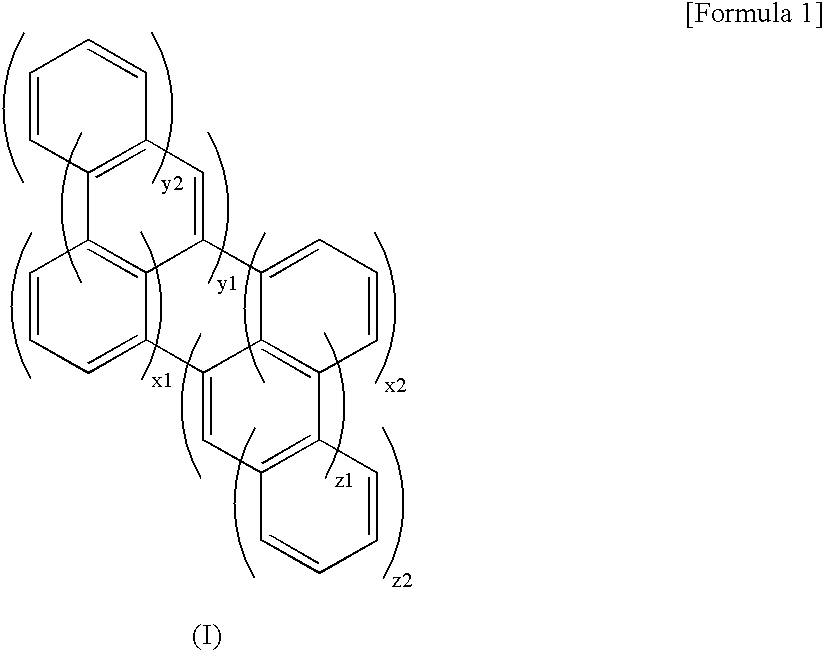
[0067]The compound was prepared according to the synthetic route 1. Specifically, naphthalene (Sigma-Aldrich Corporation) was allowed to react in NaNO2-TfOH (Tf=CF3SO2) solution, to give binaphthyl from naphthalene. Binaphthyl was allowed to react in the presence of LiTHF under oxygen bubbling, to give perylene. SbF5 purchased from Sigma-Aldrich Corporation was diluted twice under dry argon atmosphere. SO2ClF was prepared from SO2Cl2 previously prepared in halogen exchange reaction between NH4F and TFA. Perylene was allowed to react with SbF5—SO2ClF, and the product was purified by HPLC, to give dibenzoperylene. One equivalence of NCS with respect to dibenzoperylene was allowed to react with dibenzoperylene in AcOH in the presence of CHCl3 for chlorination. The product was then allowed to react with n-BuLi and Si(OC2H5)4 in THF solution, to give triethoxylsilyldibenzoperylene (yield: 8%).

[0068]Infrared absorption analysis revealed th...

example 2

Preparation of trichlorosilylcoronene

[0079]

[0080]The compound was prepared according to the synthetic route 2. Specifically, the perylene prepared in Example 1 was anionized by mixing it with an electrophilic agent in bromoacetaldehyde diethyl acetal and treated with molecular iodine, to give 1-perylene acetaldehyde diethyl acetal and its 3-isomer. The 1- and 3-perylene acetaldehyde diethyl acetals were dissolved in conc. sulfuric acid / methanol mixed solvent and ultrasonicated for 1 hour, to give benzoperylene. Similarly, the benzoperylene obtained was anionized and treated with molecular iodine, to give 5- and 7-benzoperylene acetaldehyde diethyl acetals, and these benzoperylene derivatives were ultrasonicated and purified by recrystallization from toluene, to give coronene. One equivalence of NCS with respect to the coronene was allowed to react with coronene in the presence of CHCl3 in AcOH for chlorination. The product was then allowed to react with n-BuLi and SiCl4 in THF solut...

example 3

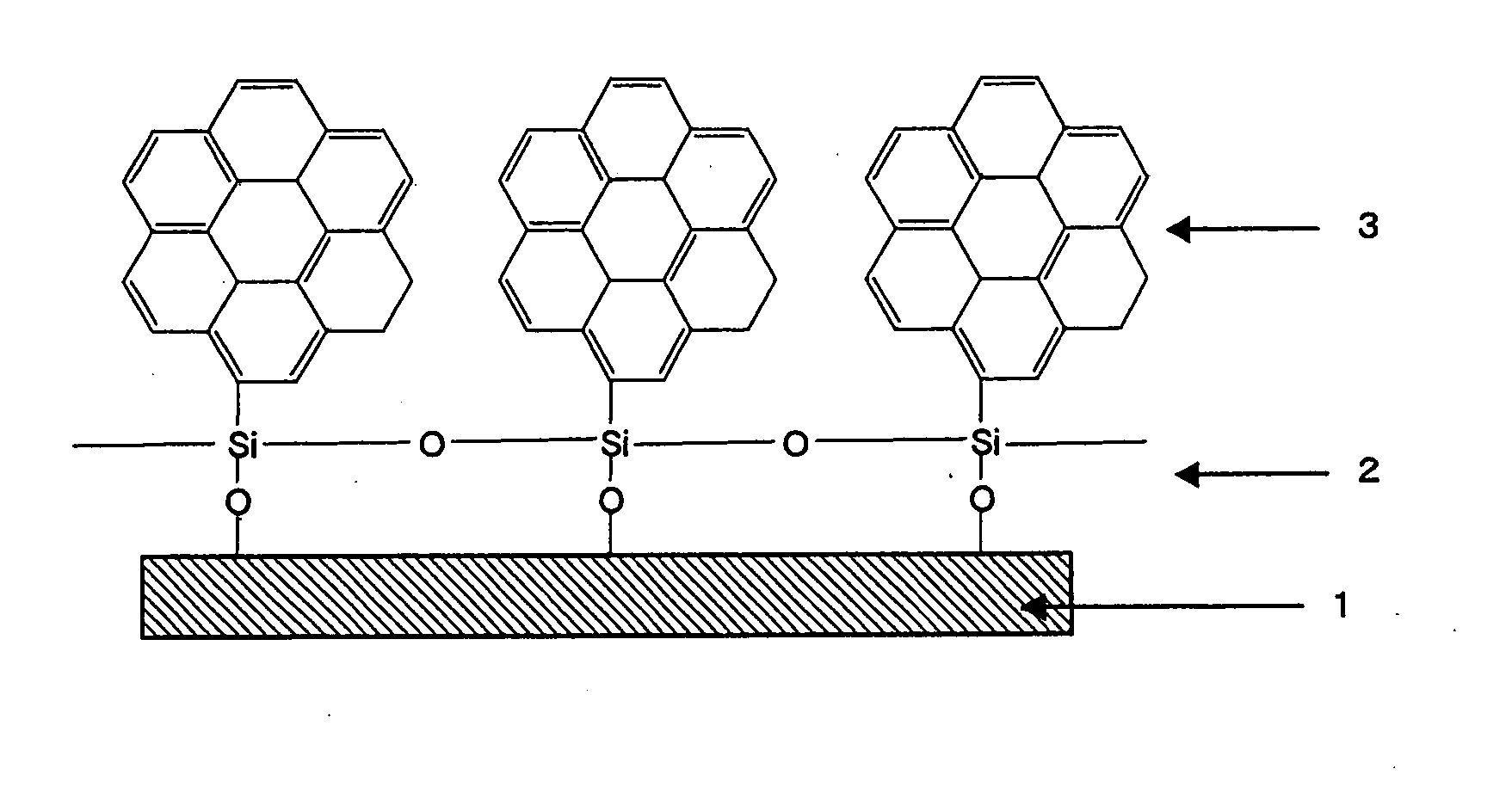
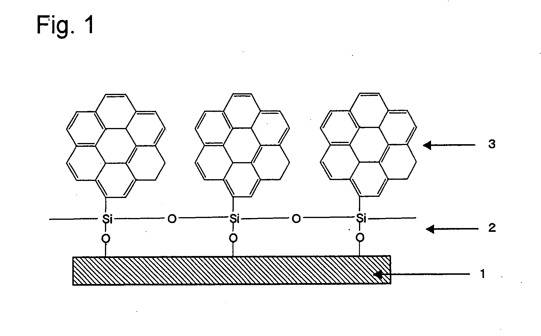
[0086]An organic thin film was formed by using the compound prepared in Example 2. Trichlorosilylcoronene was first dissolved in chloroform solvent, to give a sample solution at a concentration of 2 mM. Then, the sample solution was added dropwise in a certain amount (e.g., 100 μl) onto the water surface in a trough, forming an unimolecular film (L film) of the compound on the water surface. Pressure was applied on the water surface in that state to a particular surface pressure (e.g., 20 mN / m2), and the substrate was withdrawn at a constant speed, to form an organic thin film (LB film) shown in FIG. 1. The substrate was hydrophilized previously by immersing it in hydrogen peroxide / conc. sulfuric acid mixed solution.

[0087]AFM analysis of the trichlorosilylcoronene organic thin film formed showed a difference in height of approximately 2.6 nm. In addition, AFM and ED analysis showed periodic orientation of the constituent atoms on the film, indicating that an oriented organic thin fi...


PUM

PropertyMeasurementUnit
hydrophobicaaaaaaaaaa
band gapaaaaaaaaaa
solubleaaaaaaaaaa

Abstract

The present invention provides a highly ordered, crystallized organic thin film superior in electroconductive properties that is resistant to exfoliation, a compound for preparation of the thin film, and a method of producing the same.An organic silane compound, characterized in that a molecule represented by General Formula (I) is substituted with a silyl group.A method of producing the organic silane compound, comprising halogenating a molecule (I) and allowing it to react with a silane derivative.An organic thin film, wherein the organic silane compound molecule is oriented with its silyl group located in the substrate side and the molecule (I) region in the film surface side.(wherein, x1 and x2 are integers satisfying 1≦x1, 1≦x2, and 2≦x1+x2≦8; each of y1 and z1 is independently an integer of 2 to 8; each of y2 and z2 is independently an integer of 0 to 8; and the skeleton may be substituted with a hydrophobic group).

Description

TECHNICAL FIELD[0001]The invention relates to an organic silane compound, a method of producing the compound, and an organic thin film using the compound.BACKGROUND ART[0002]Recently under progress is research and development on semiconductors of organic compound, because these semiconductors are simpler in production than semiconductors of inorganic material, allow cost down by mass production, and have functions wider in variety than those from an inorganic material, and such organic semiconductors have been reported.[0003]The compound most intensively studied as a material for organic devices is pentacene. It is because pentacene, which has a very small band gap and a rigid structure, can be used for production of organic devices with superior characteristics, if it is highly oriented. Vacuum deposition has been used as a method of forming such a pentacene thin film. It is because pentacene is scarcely soluble in solvent and thus it was difficult to form a thin film in a solution...

Claims


Application Information

Patent Timeline
Patent Type & Authority Applications(United States)
IPC IPC(8): C07F7/02
CPCC07F7/12C07F7/1836H01B1/12H01L51/0012H01L51/0056H01L51/0094C07F7/1804H10K71/191H10K85/624H10K85/40
Inventor IMADA, HIROSHIHANATO, HIROYUKITAMURA, TOSHIHIRO
Owner SHARP KK
Why Eureka
Try Eureka