Light emitting diode, optoelectronic device and method of fabricating the same

Inactive Publication Date: 2008-12-25
NAT CENT UNIV
View PDF2 Cites 16 Cited by
  • Summary
  • Abstract
  • Description
  • Claims
  • Application Information

AI Technical Summary

Benefits of technology

[0010]Accordingly, the present invention provides a light emitting diode structure and a method of fabricating the same. To produce the light emitting diode structure, a strain-reducing seed layer is formed on a substrate. Thereafter, the required high temperature gallium nitride epitaxial lay

Problems solved by technology

The high dislocation density can have some adverse effects on the property and performance of the light emitting diode 100.
However, the clusters formed by the silicon nitrid

Method used


Image

  • Light emitting diode, optoelectronic device and method of fabricating the same
  • Light emitting diode, optoelectronic device and method of fabricating the same
  • Light emitting diode, optoelectronic device and method of fabricating the same

Examples


Embodiment Construction

[0036]Reference will now be made in detail to the present preferred embodiments of the invention, examples of which are illustrated in the accompanying drawings. Wherever possible, the same reference numbers are used in the drawings and the description to refer to the same or like parts.

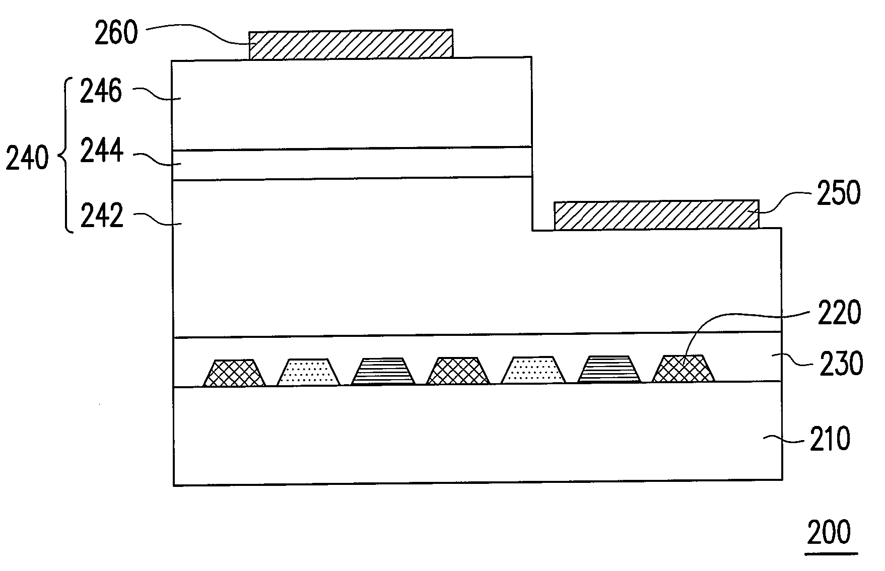
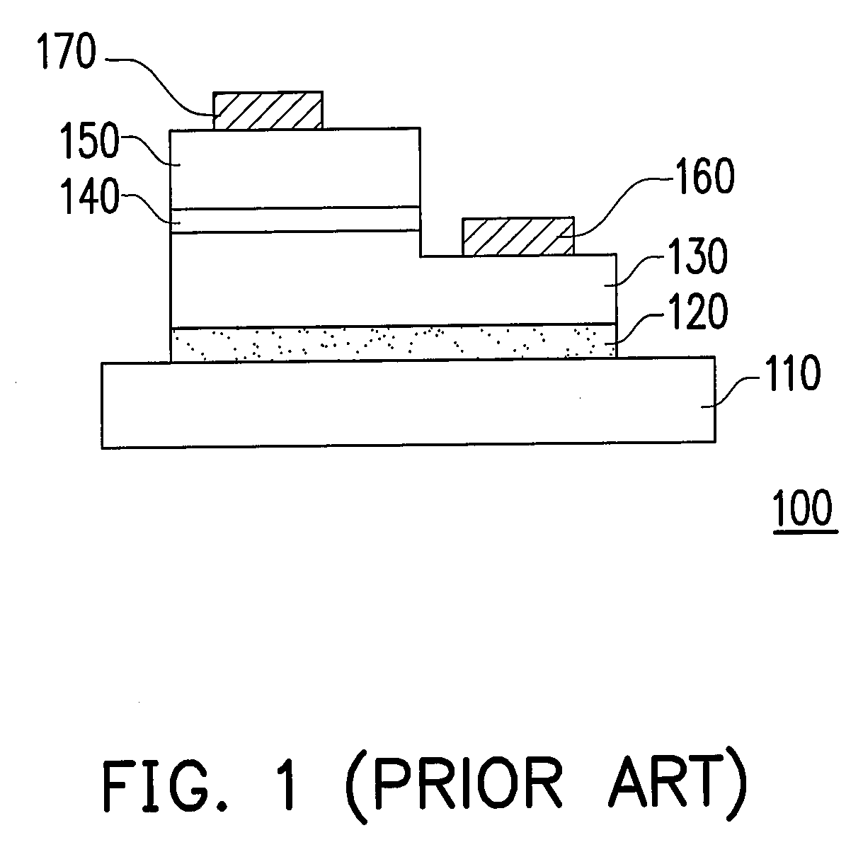
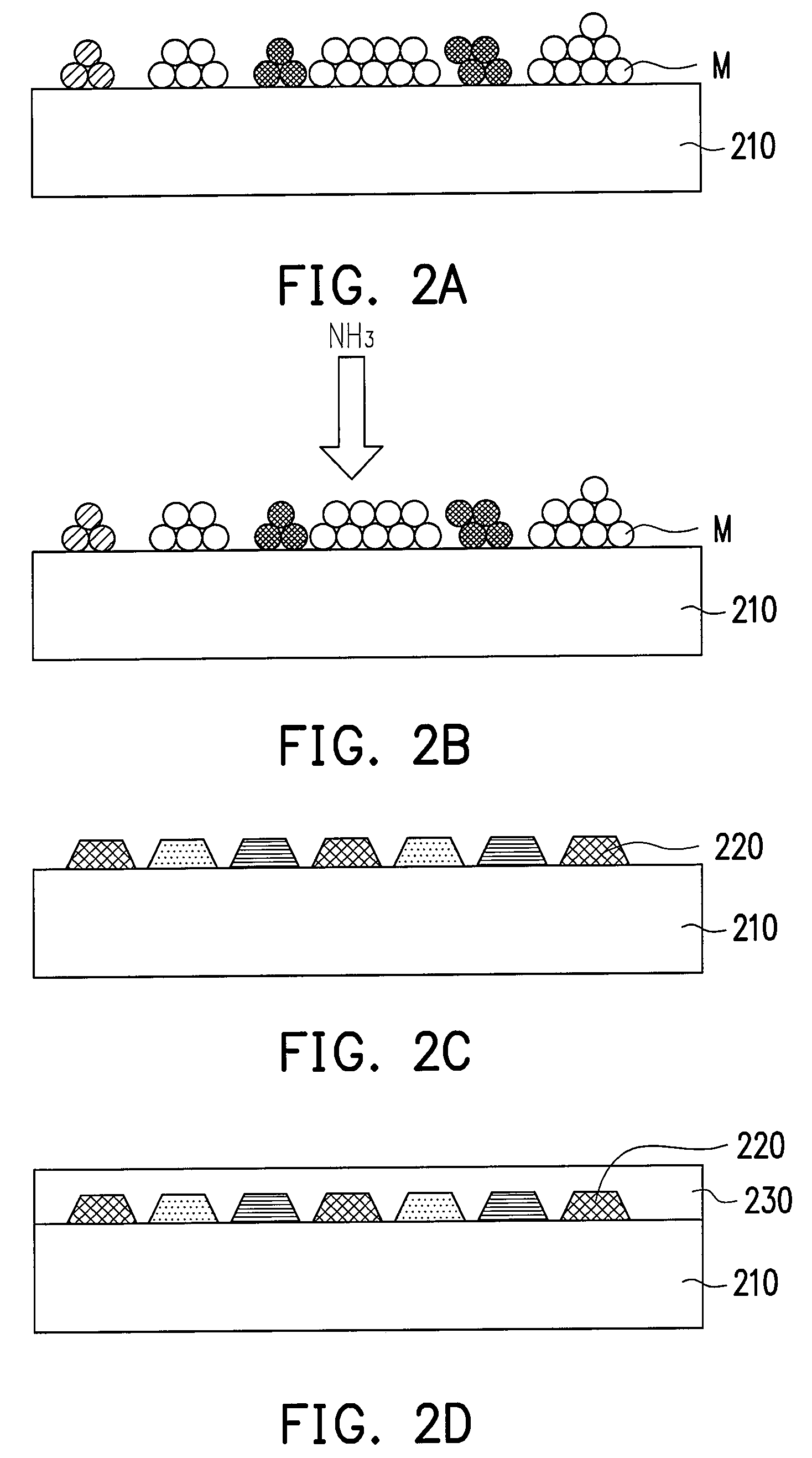
[0037]FIGS. 2A to 2F are schematic cross-sectional views showing the steps in a method of fabricating a light emitting diode structure according to the present invention. First, as shown in FIG. 2A, a substrate 210 is provided. Then, a metallic material M is spread on the substrate 210. The metallic material M is selected from a group consisting of aluminum, magnesium and indium. The substrate 210 can be fabricated using a material selected from a group consisting of silicon, glass, gallium arsenide, gallium nitride, aluminum-gallium arsenide, gallium phosphide, silicon carbide, indium phosphide, boron nitride, zinc oxide, aluminum oxide, lithium aluminate and aluminum nitride. In the present embodim...


PUM


Abstract

A light emitting diode structure including a substrate, a strain-reducing seed layer, an epitaxial layer, a first electrode and a second electrode is provided. The strain-reducing seed layer having a plurality of clusters is disposed on the substrate, and the material of the clusters is selected from a group consisting of aluminum nitride, magnesium nitride and indium nitride. The epitaxial layer includes a first type doped semiconductor layer, a light emitting layer and a second type doped semiconductor layer. The first electrode is disposed on the exposed first type doped semiconductor layer and electrically connected thereto. The second electrode is disposed on the second type doped semiconductor layer and electrically connected thereto.

Description

CROSS-REFERENCE TO RELATED APPLICATION[0001]This application claims the priority benefit of Taiwan application serial no. 96122017, filed on Jun. 20, 2007. The entirety of the above-mentioned patent application is hereby incorporated by reference herein and made a part of specification.BACKGROUND OF THE INVENTION[0002]1. Field of the Invention[0003]The present invention generally relates to a light emitting diode structure and method of fabricating the same, and more particularly, to a light emitting diode structure having a strain-reducing seed layer for reducing the dislocation density thereof and a method of fabricating the same.[0004]2. Description of Related Art[0005]Light emitting diode is a semiconductor device used in a light emitting device. Because of low power consumption, low contamination, long working life, and rapid responding speed, light emitting diode is useful in many areas such as traffic bulletin boards, outdoor display panels and the back light of displays. The...

Claims


Application Information

Patent Timeline
IPC IPC(8): H01L33/00H01L21/00H01L33/12
CPCH01L33/007H01L33/12
Inventor KUO, CHENG-HUANGLAI, WEI-CHIHKUO, CHI-WEN
Owner NAT CENT UNIV
Why Eureka
Try Eureka