Semiconductor device

a technology of semiconductor devices and semiconductors, applied in the direction of semiconductor devices, basic electric elements, electrical appliances, etc., can solve the problems of affecting the efficiency of semiconductor devices, the trade-off between device breakdown voltage and on-resistance, and the disadvantage of high-breakdown voltage devices

Inactive Publication Date: 2008-12-25
KK TOSHIBA
View PDF7 Cites 58 Cited by
  • Summary
  • Abstract
  • Description
  • Claims
  • Application Information

AI Technical Summary

Benefits of technology

[0012]In one aspect the present invention provides a semiconductor device having a drift layer with a pillar structure including first semiconductor layer portions of the first conduction type and second semiconductor layer portions of the second conduction type formed in pillars alternately and periodically on a semiconductor substrate, the device comprising: a device region including a plurality of transistors composed of the first semiconductor layer portions and the second semiconductor layer portions and arrayed in the central area of the semiconductor device; and a terminal region formed at the periphery of the device region without the transistors formed therein, wherein the drift layer in the terminal region has a resistance controlled higher than the resistance of the drift layer in the device region and higher than the resistance determined by an impurity concentration.

Problems solved by technology

On the other hand, as it has no conductivity modulation, it is more disadvantageous in high-breakdown voltage devices from the viewpoint of the on-resistance than bipolar devices such as an IGBT (Insulated Gate Bipolar Transistor).
Therefore, there is a tradeoff between the device breakdown voltage and the on-resistance.
This causes a problem because the entire semiconductor device may be broken down.
In this case, if only the breakdown voltage in the terminal region is enhanced higher than that in the device region, the carrier excessively stored in the terminal region can not be discharged sufficiently on reverse recovery of the internal diode in the transistor in the device region.

Method used


Image

  • Semiconductor device
  • Semiconductor device
  • Semiconductor device

Examples


first embodiment

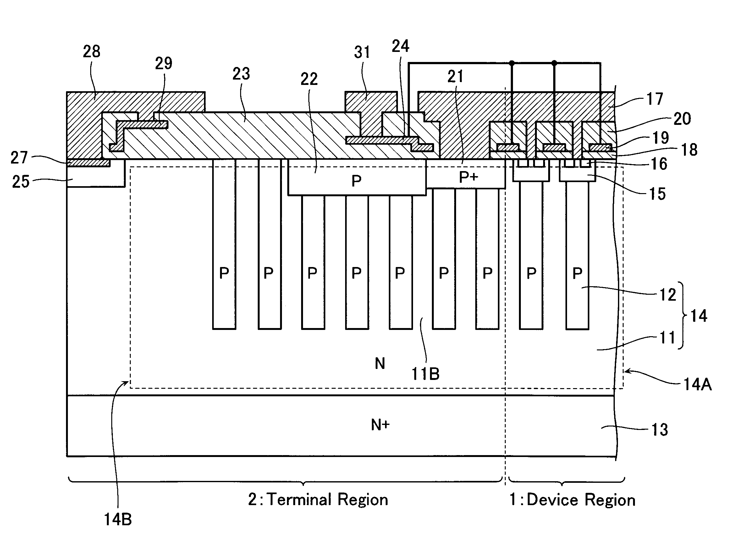
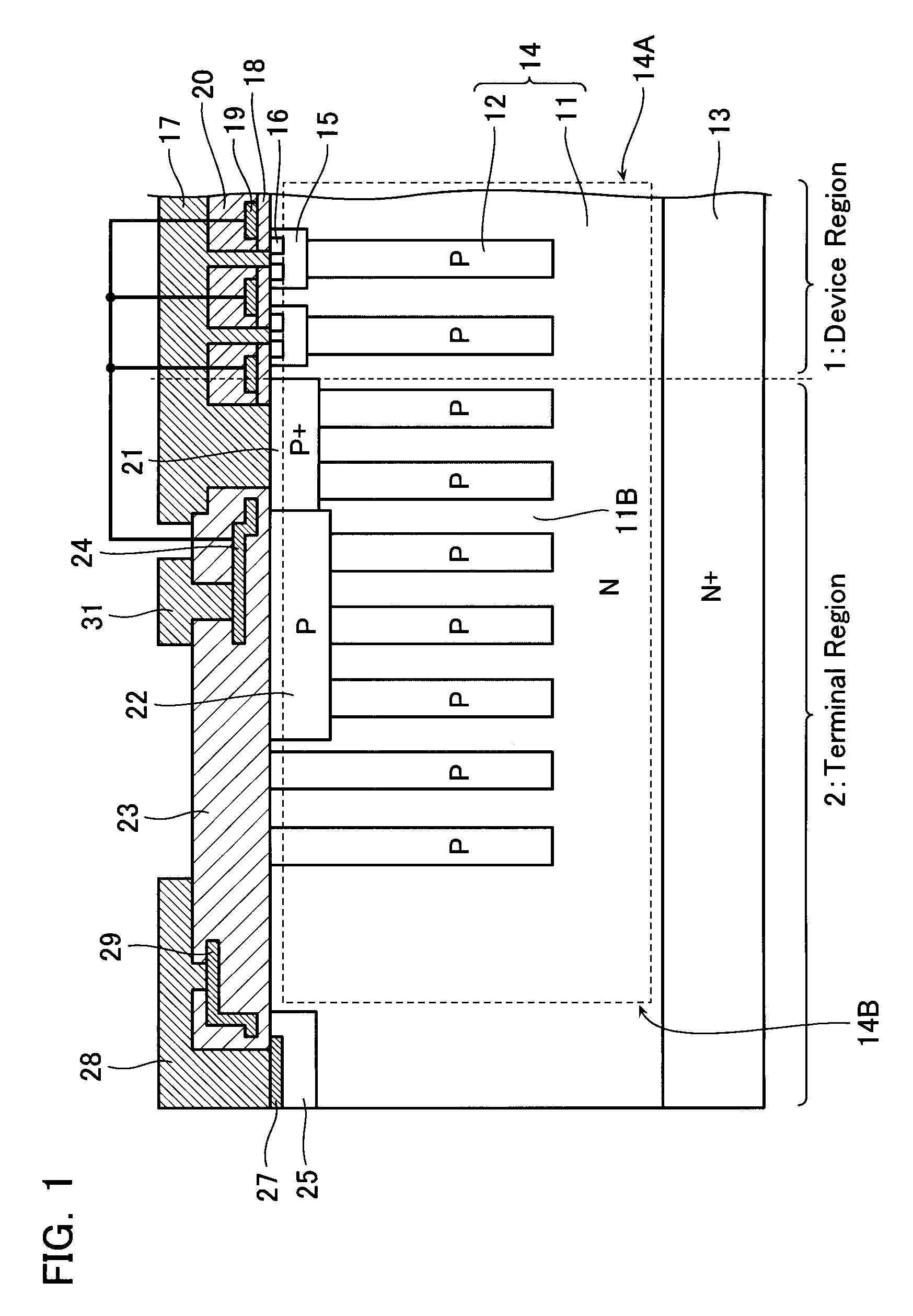
[0022]One embodiment in the present invention will now be described below. A semiconductor device in the present embodiment is shown in FIG. 1. The semiconductor device in the present embodiment is a power semiconductor device, which comprises a device region 1 and a terminal region 2.

[0023]A transistor formed in the device region 1 has a superjunction structure, which includes an N-type drift layer 11, and a plurality of P-type pillar layer portions 12 formed in the N-type drift layer 11. The N-type drift layer 11 has one surface (the lower surface in FIG. 1), on which an N+-type drain layer 13 is formed with a higher impurity concentration than the N-type drift layer 11. A drain electrode, not shown, is formed on the surface of the N+-type drain layer 13. In the present embodiment, a drift layer 14 includes the N-type drift layer 11 and the P-type pillar layer 12, and the drift layer 14 has a drift layer 14A formed in the device region 1 and a drift layer 14B formed in the termina...

second embodiment

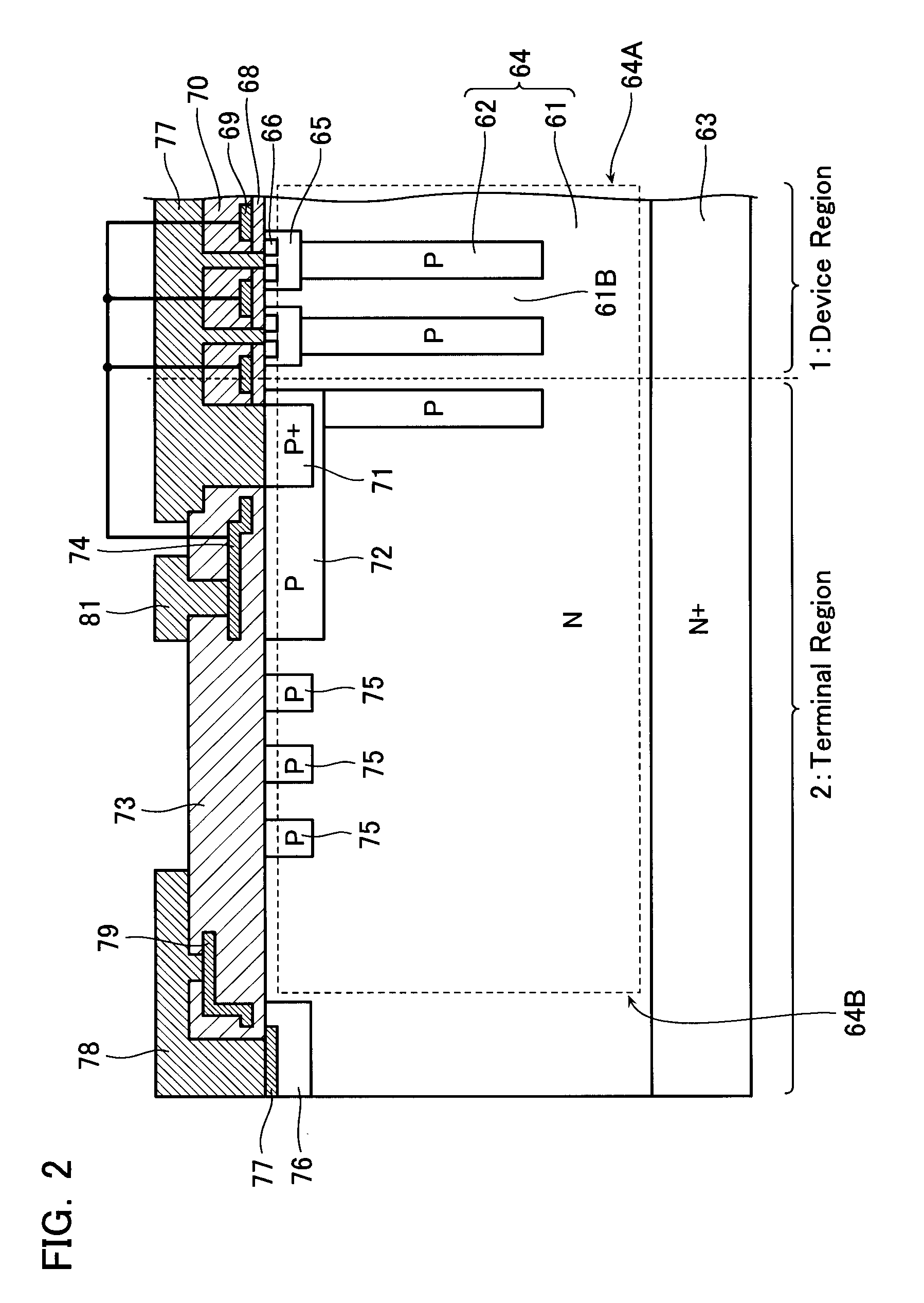
[0036]A second embodiment in the present invention is described below. A semiconductor device in the present embodiment is shown in FIG. 2. The semiconductor device in the present embodiment is a power semiconductor device, which comprises a device region 51 and a terminal region 52.

[0037]A transistor formed in the device region 51 has a superjunction structure, which includes an N-type drift layer 61, and a plurality of P-type pillar layer portions 62 formed in the N-type drift layer 61. In this embodiment, preferably, the P-type pillar layer 62 reaches the bottom of the N-type drift layer as shown in FIG. 2.

[0038]The N-type drift layer 61 has one surface (the lower surface in FIG. 2), on which an N+-type drain layer 63 is formed with a higher impurity concentration than the N-type drift layer 61. A drain electrode, not shown, is formed on the surface of the N+-type drain layer 63. In the present embodiment, a drift layer 64 includes the N-type drift layer 61 and the P-type pillar ...


PUM


Abstract

There is provided a semiconductor device having a drift layer with a pillar structure including first semiconductor layer portions of the first conduction type and second semiconductor layer portions of the second conduction type formed in pillars alternately and periodically on a semiconductor substrate. A device region includes a plurality of arrayed transistors composed of the first semiconductor layer portions and the second semiconductor layer portions. A terminal region is formed at the periphery of the device region without the transistors formed therein. The drift layer in the terminal region has a carrier lifetime lower than ⅕ the carrier lifetime in the drift layer in the device region.

Description

CROSS-REFERENCE TO RELATED APPLICATION[0001]This application is based upon and claims the benefit of priority from prior Japanese Patent Application No. 2007-165797, filed on Jun. 25, 2007, the entire contents of which are incorporated herein by reference.BACKGROUND OF THE INVENTION[0002]1. Field of the Invention[0003]The present invention relates to a semiconductor device, and more particularly to a power semiconductor device with a high-breakdown voltage structure.[0004]2. Description of the Related Art[0005]In response to the needs in the field of recent power electronics for downsized high-performance power supplies, effort is put into improving performances to achieve high-breakdown voltage / large-current and low-loss / high-speed power semiconductor devices. Of those, a power MOSFET (Metal Oxide Semiconductor Field Effect Transistor) has a high-speed switching performance and becomes established as a key device in the field of switching power supplies and so forth.[0006]The MOSFE...

Claims


Application Information

Patent Timeline
Patent Type & Authority Applications(United States)
IPC IPC(8): H01L29/78
CPCH01L21/26513H01L21/26586H01L29/0615H01L29/0619H01L29/0634H01L29/1095H01L29/167H01L29/32H01L29/402H01L29/66712H01L29/7811
Inventor TAKASHITA, MASAKATSUSUMI, YASUTOIZUMISAWA, MASARUOHTA, HIROSHISAITO, WATARUONO, SYOTARO
Owner KK TOSHIBA
Why Eureka
Try Eureka