Electrode of aluminum-alloy film with low contact resistance, method for production thereof, and display unit

a technology of aluminum alloy and contact resistance, which is applied in the direction of electrical devices, semiconductor devices, instruments, etc., can solve the problems of defective display (defective glowing) and uneven image display in the display unit, and achieve the effect of reducing contact resistance and minimizing the number of pixel errors in the display uni

Inactive Publication Date: 2009-01-01
KOBE STEEL LTD
View PDF26 Cites 42 Cited by
  • Summary
  • Abstract
  • Description
  • Claims
  • Application Information

AI Technical Summary

Benefits of technology

[0029]According to the present invention, the aluminum alloy film is given surface roughness by wet etching with an alkaline solution or dry etching with a mixed gas of SF6 and Ar, so that the alloying element precipitates on its surface. The result is a reduced contact resistance despite a small amount of alloying element, and this minimizes the number of pixel errors in the display unit.

Problems solved by technology

Liquid crystal panels that have recently become larger than before pose a problem with uneven image display due to resistance of wiring between the gate electrode and the source-drain electrodes and ensuing delay in voltage pulse propagation.
The gate electrode and the source-drain electrodes of high contact resistance with the visible light transparent conductive film cause a trouble of defective display (defective glowing) in the display unit.

Method used


Image

  • Electrode of aluminum-alloy film with low contact resistance, method for production thereof, and display unit
  • Electrode of aluminum-alloy film with low contact resistance, method for production thereof, and display unit
  • Electrode of aluminum-alloy film with low contact resistance, method for production thereof, and display unit

Examples


example 1

[0062]A non-alkali glass plate (0.7 mm thick) as a substrate was coated by sputtering with a thin film of aluminum alloy (varying in composition) which functions as the gate electrode and the source-drain electrodes. The aluminum alloy contains Al, Ni (0.2-1.0 atom %), and La (0.1-0.5 atom %). The thin film is about 300 nm thick. The coated glass plates were used as samples.

[0063]The samples were divided into four groups (A to D). The samples of Group A (designated as Test Nos. 1 to 3 in Table 1 given later) were left as such, and the samples of Group D (designated at Test Nos. 15 to 22 in Table 1) underwent wet etching with an alkaline solution (an aqueous solution, pH 9-13, of resist remover “TOK106” from TOKYO OHKA KOGYO CO., LTD.).

[0064]The aluminum alloy thin film, with or without etching (in both Group A and Group D), underwent photolithography and etching for patterning. This etching was performed such that the aluminum alloy thin film has its edge sloped about 30-40°. On the...

example 2

[0070]A non-alkali glass plate (0.7 mm thick) as a substrate was coated by sputtering with a thin film of aluminum alloy which functions as the gate electrode and the source-drain electrodes. The aluminum alloy contains Al and Ni (0.22 atom %). The thin film is about 300 nm thick. The coated glass plate was used as a sample.

[0071]The aluminum alloy thin film on the sample underwent wet etching with an aqueous solution, pH 9-13, of resist remover “TOK106” from TOKYO OHKA KOGYO CO., LTD. Duration of wet etching was varied so as to control the amount of etching. The thus treated samples were examined for contact resistance in the same way as in Example 1. They were also examined for surface roughness at interface between the transparent conductive film and the aluminum alloy thin film (in terms of maximum height Rz according to JIS B0601 (2001)). The results are shown in Table 2. (The symbol “-” means no data available.) The data in Table 2 are graphed in FIG. 13 to represent the relat...

example 3

[0073]A non-alkali glass plate (0.7 mm thick) as a substrate was coated by sputtering with a thin film of aluminum alloy which functions as the gate electrode and the source-drain electrodes. The aluminum alloy contains Al, Ni (0.3 atom %), and La (0.35 atom %). The thin film is about 300 nm thick. The coated glass plate was used as a sample.

[0074]Each sample was processed in the same way as in Example 1 to form a contact hole (with an area of 10×10 μm) in the silicon nitride film and then underwent dry etching with a mixed gas composed of SF6 (33.3%), O2 (26.7%), and Ar (40%) or a mixed gas composed of SF6 (60%) and Ar (40%). The dry etching was reactive ion etching (RIE). It also varied in duration from level 1 to level 3 as defined below. After standing for 8 hours, the surface of the aluminum alloy thin film was coated by sputtering with an ITO film, 200 nm thick.

Etching level 1: twice the duration necessary to remove the silicon nitride film formed on the aluminum alloy film.

Et...


PUM

PropertyMeasurementUnit
surface roughnessaaaaaaaaaa
depthaaaaaaaaaa
height Rzaaaaaaaaaa

Abstract

Disclosed herein are an electrode of aluminum alloy film, a method for production thereof, and a display unit provided therewith, said electrode exhibiting a low electric resistance when in contact with a transparent oxide conductive film even though the aluminum alloy contains a less amount of alloying element than usual. The electrode of low contact resistance type is an aluminum alloy film in direct contact with a transparent oxide electrode, wherein said aluminum alloy film contains 0.1-1.0 atom % of metal nobler than aluminum and is in direct contact with a transparent oxide electrode through a surface having surface roughness no smaller than 5 nm in terms of maximum height Rz.

Description

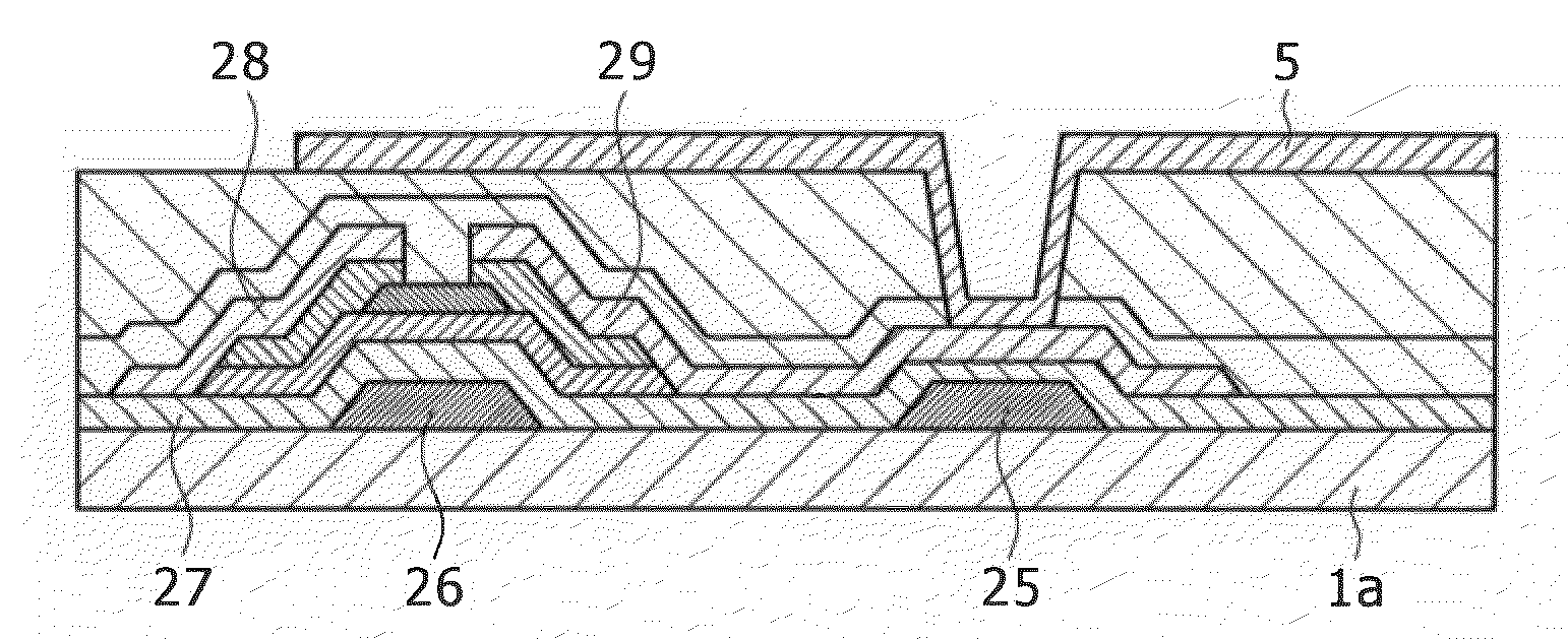
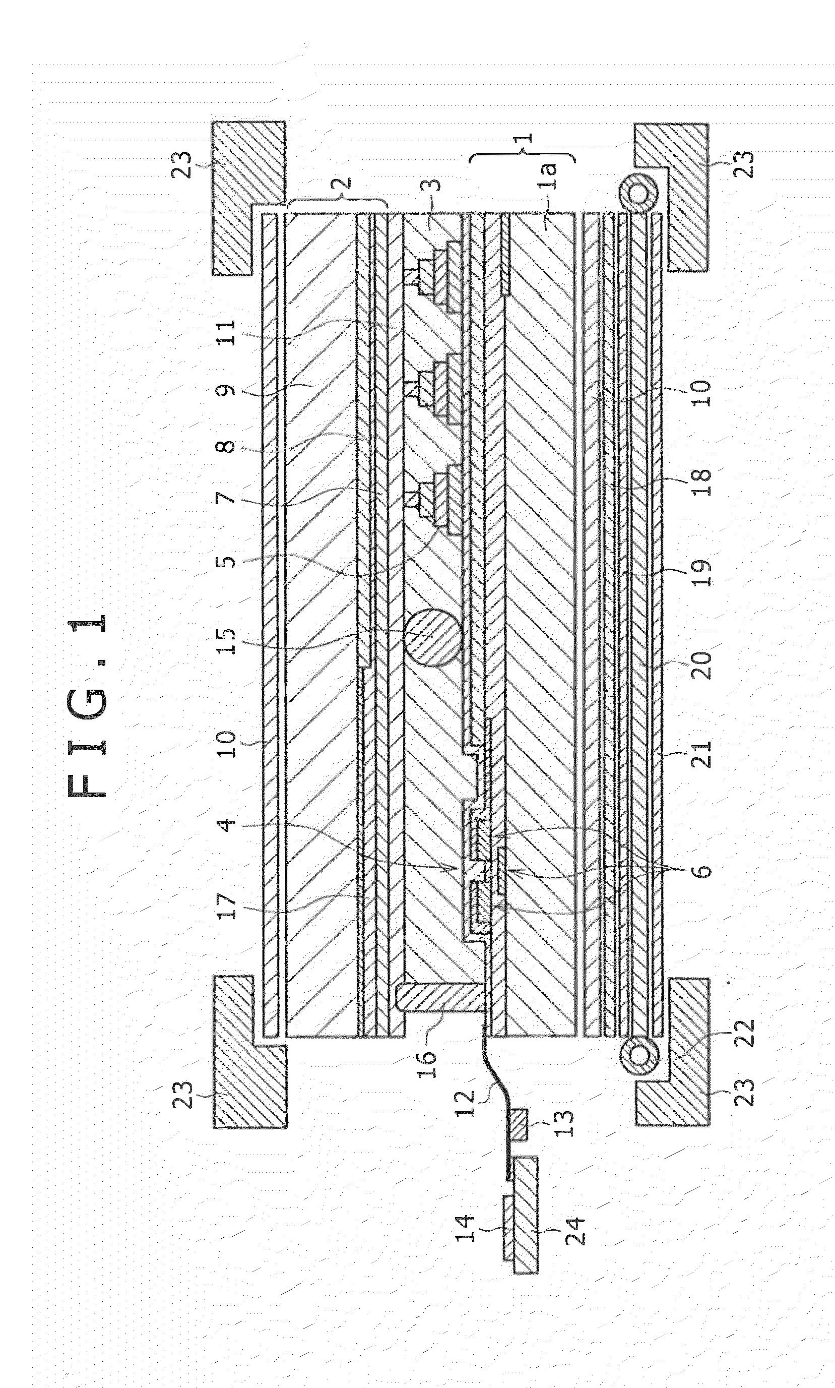
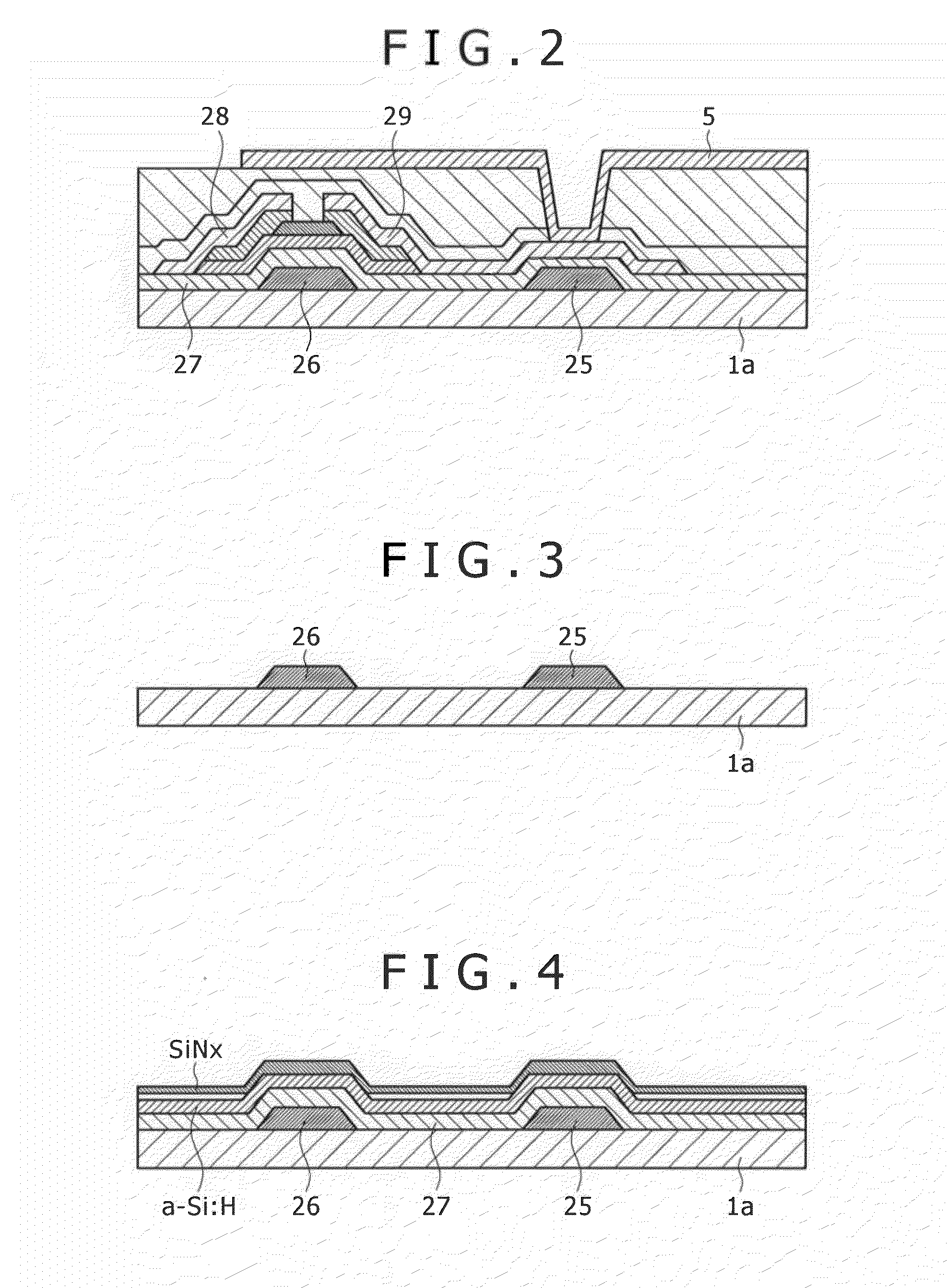
BACKGROUND OF THE INVENTION[0001]1. Field of the Invention[0002]The present invention relates to an electrode of aluminum-alloy film, a method for production thereof, and a display unit provided therewith, the electrode having a low contact resistance and finding use in flat electronic display units typified by liquid crystal display units.[0003]2. Description of the Related Art[0004]Liquid crystal display units find use in broad applications ranging from small portable telephones to large televisions exceeding 30 inches. They fall under two classes—simple matrix type and active matrix type—according to the pixel driving method. The latter employs thin film transistors (TFT) as switching elements and is in general use because of its ability to produce high-quality images.[0005]FIG. 1 is a schematic enlarged sectional view showing the structure of a typical liquid crystal panel used for the liquid crystal display unit of active matrix type. The shown liquid crystal panel is composed ...

Claims


Application Information

Patent Timeline
Patent Type & Authority Applications(United States)
IPC IPC(8): H01L29/04H01L21/28
CPCH01L27/124H01L29/458G02F1/136227G02F1/136286H01L27/1214
Inventor OCHI, MOTOTAKAGOTOU, HIROSHIOKUNO, HIROYUKITAKETOMI, YUICHI
Owner KOBE STEEL LTD
Why Eureka
Try Eureka