

Fine resist pattern forming method and nanoimprint mold structure
a nano-imprint mold and pattern technology, applied in the field of fine resist pattern forming method and nano-imprint mold structure, can solve the problems of high degree of technical difficulty, mold pattern needs to be formed with a high precision, and no lithography tool can mass-produce an lsi at hp 32 nm or less, etc., to achieve simple process method, high precision, and low cost
- Summary
- Abstract
- Description
- Claims
- Application Information
AI Technical Summary
Benefits of technology
Problems solved by technology
Method used
Image

Examples
Embodiment Construction
[0022]Hereinafter, exemplary embodiments of the present invention will be described in detail with reference to drawings.
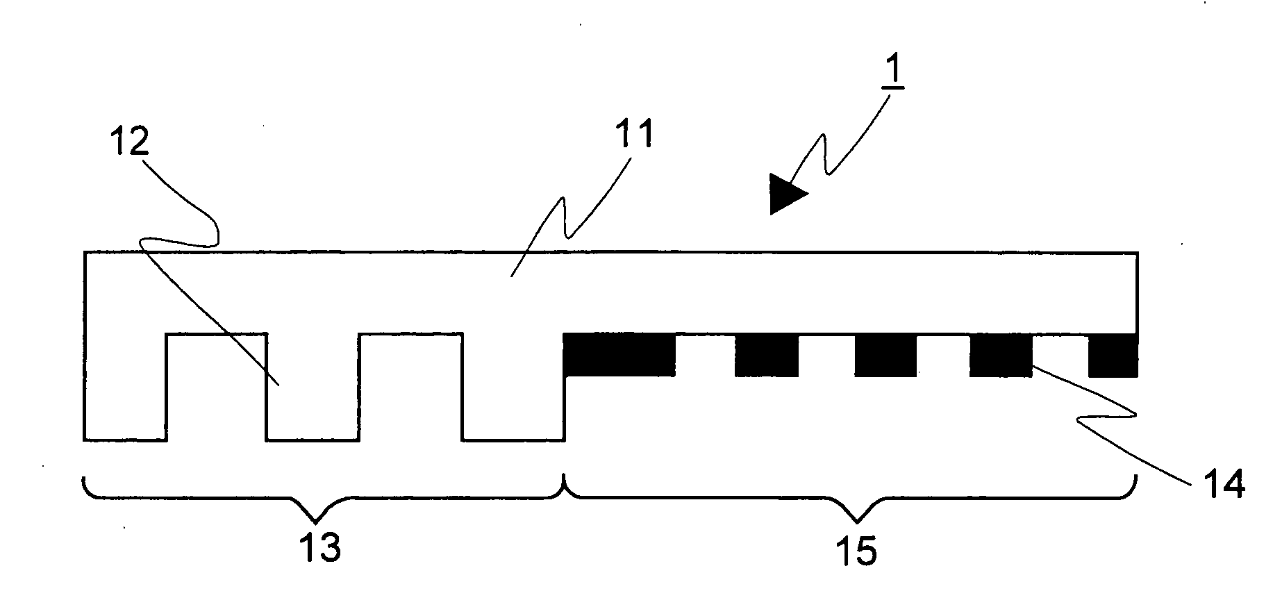
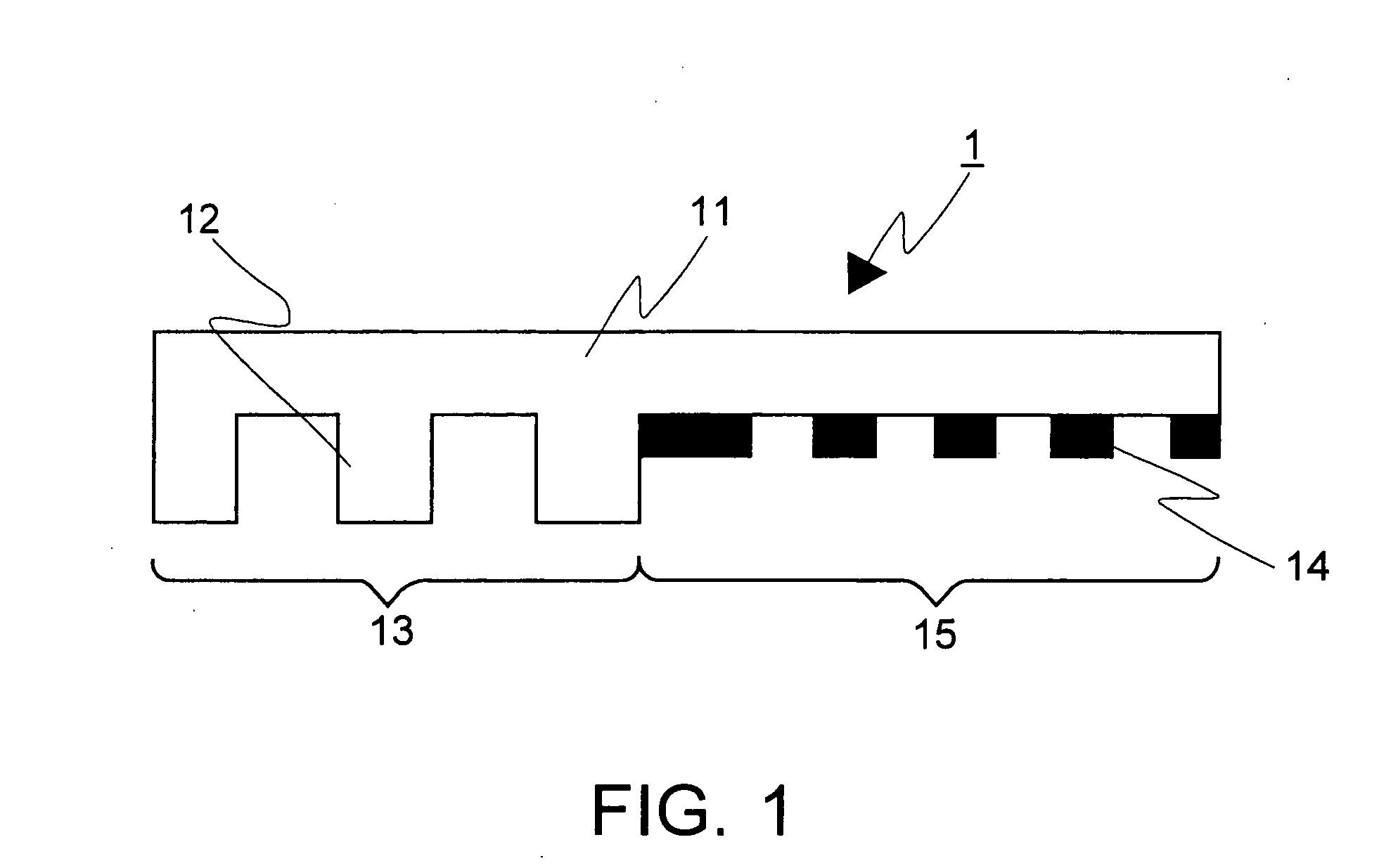
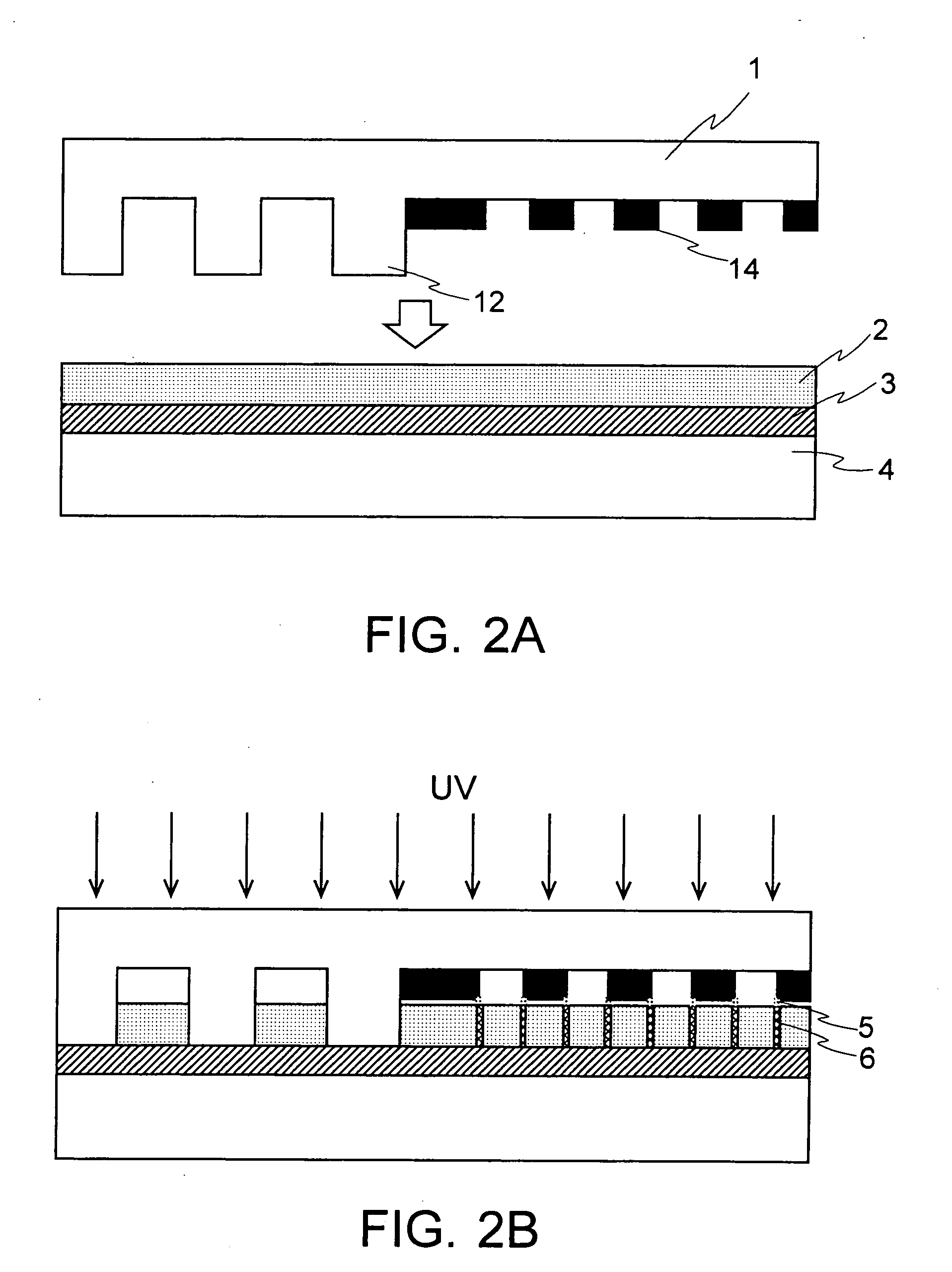
[0023]FIG. 1 is a rough cross-sectional view of mold structure (hereinafter referred to as mold) 1 in accordance with the present invention. Mold 1 is formed such that the surface of glass material substrate 11 such as glass and quartz allowing nonresonant light, such as UV light, (hereinafter referred to as UV light, but not limited to this) of a wavelength band other than the photosensitive band of a photoresist to pass through is formed into a concave-convex surface. Convex portion 12 constitutes nanoimprint pattern portion 13, and conductive film pattern 14 formed in consecutive concave portions constitutes nonadiabatic near-field light exposure pattern portion 15.
[0024]In order to perform transfer onto a resist film formed on a workpiece substrate using mold 1, press convex portion 12 of mold 1 so as to pass through a resist film, irradiate UV light from the ...
PUM
| Property | Measurement | Unit |
|---|---|---|
| width | aaaaa | aaaaa |
| wavelength | aaaaa | aaaaa |
| width | aaaaa | aaaaa |
Abstract
Description
Claims
Application Information