Optical transmitter and method for control the same

a technology of optical transmitter and optical control, applied in the field of optical transmitter, can solve the problems of affecting the transmission status, saturation of amplifier, and scattering of stimuli within the transmission fiber, and achieve the effect of reducing both the transient chirp and the stimulated

Inactive Publication Date: 2009-01-01
SUMITOMO ELECTRIC IND LTD
View PDF4 Cites 25 Cited by
  • Summary
  • Abstract
  • Description
  • Claims
  • Application Information

AI Technical Summary

Benefits of technology

[0006]Therefore, one aspect of the present invention is to provide an optical transmitter that reduces both the transient chirp and the stimulated Brillouin scattering occurred within the transmission optical fiber, and to provide a method to control the optical transmitter.

Problems solved by technology

However, when the laser diode is free from the modulation, that is, the modulation signal provided to the transmitter becomes off, an optical signal with a quite large peak power and a narrow spectrum enters the optical fiber, which causes the stimulated Brillouin scattering within the transmission fiber.
Once the Brillouin scattering occurs, the optical power reaching the optical amplifier that is ordinarily installed in the midway of the transmission line decreases and the optical amplifier tries to adjust its optical gain so as to keep the optical output therefrom constant, which causes the saturation of the amplifier, or affects the transmission status of the normally operating signal channels in the wavelength division multiplexing (WDM) system.

Method used


Image

  • Optical transmitter and method for control the same
  • Optical transmitter and method for control the same
  • Optical transmitter and method for control the same

Examples


first embodiment

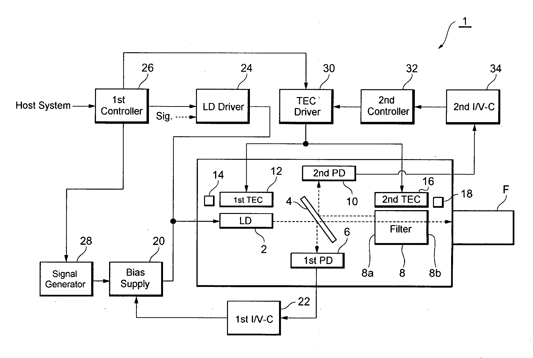
[0019]FIG. 1 schematically illustrates a functional block diagram of an optical transmitter according to the first embodiment of the invention. The optical transmitter 1, which is one type of the CML device, comprises an LD 2, an optical splitter 4, a first photodiode (hereafter denoted as PD) 6, an optical filter 8, a second PD 10, a first thermo-electric cooler (hereafter denoted as TEC) 12, a first thermistor 14, a second TEC 16 and a second thermistor 18. This optical transmitter 1 may electrically communicate with a host system, and may optically couple with an optical fiber F.

[0020]The LD 2 is a type of, what is called, a distributed feedback laser diode (DFB-LD), and may emit the light by being provided with a bias current supplied from the bias unit 20. The signal light output from the LD 2 enters the optical fiber F passing through the optical splitter 4 and the optical filter 8. The optical splitter 4, arranged on the optical axis between the LD 2 and the optical fiber F, ...

second embodiment

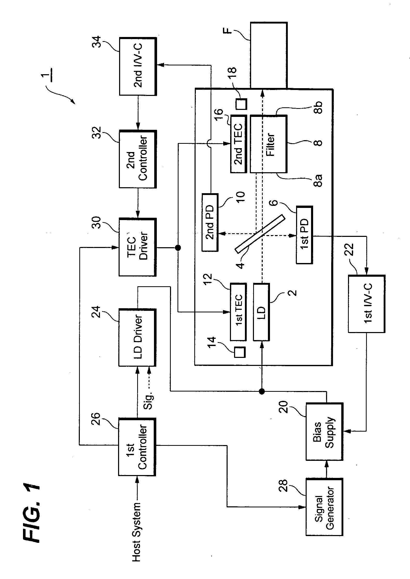
[0034]Next, a second embodiment of the optical transmitter 1a according to the present invention will be described. FIG. 3 schematically illustrates a functional block diagram of the optical transmitter 1a. This optical transmitter 1a further comprises a first detector 36 in addition to those of the first transmitter 1 shown in FIG. 1. The first detector 36 includes a peak / bottom detector 36a and the first comparator 36b. The first I / V-C 22 outputs the voltage signal corresponding to the first photocurrent generated by the first PD 6 to both the bias unit 20 and the peak / bottom detector 36a.

[0035]The peak / bottom detector 36a monitors the peak value and the bottom value of the voltage signal provided from the first I / V-C 22 with a preset period, and calculates the time variation of the difference between the peak and the bottom values, which we call the first variation. This first variation reflects the variation of the difference between the maximum and the minimum output power emi...

third embodiment

[0041]Next, the third embodiment of the optical transmitter according to the present invention will be described as referring to FIG. 5 that schematically illustrates the functional block diagram of the optical transmitter 1b. This optical transmitter 1b further comprises a second detector 38 in addition to those provided in the first transmitter shown in FIG. 1. The second detector 38 includes a calculating unit 38a and the second comparator 38b. The second I / V-C 43 converts the second photocurrent generated by the second PD 10 into the voltage signal and sends this voltage signal to both the second controller 32 and the calculating unit 38a.

[0042]The calculating unit 38a calculates a time variation, which we call as the second variation, of the voltage signal sent from the second I / V-C 34. The second variation indicates the time variation of the light reflected by the optical filter 8 which is monitored by the second PD 10. The calculating unit 38a sends the second variation to t...


PUM


Abstract

An optical transmitter that reduces the stimulated Brillion scattering occurred within a transmission optical fiber and a method to control the optical transmitter are disclosed. The optical transmitter with a type of the chirp managed laser diode (CML) comprises a laser diode modulated with a high frequency signal and biased with a relatively large bias current and an optical filter. When the modulation signal is stopped, an optical signal with relatively large power and narrow spectrum may enter the transmission fiber, which causes the stimulated Brillouin scattering. In the present optical transmitter, when the modulation signal is absent, an auxiliary signal is superposed on the bias current.

Description

BACKGROUND OF THE INVENTION[0001]1. Field of the Invention[0002]The present invention relates to an optical transmitter and a method to control this optical transmitter.[0003]2. Related Prior Arts[0004]It has been known that an optical communication system with relatively long distance will be realized by the CML technique, “Chirp managed directly modulated laser diode”, that effectively reduces the transient chirp. Matsui, et al. and Mahgerefteh, et al. have reported this technique in IEEE Photonics Technology Letters, p 385, vol. 18 (2), Jan. 15, 2006 and Electronics Letters, vol. 41(9), Apr. 28, 2005, respectively. This CML technique may reduce the transient chirp by directly driving a laser diode (hereafter denoted as LD) with relatively large bias current and relatively small modulation current, and may secure an extinction ratio by cutting optical components corresponding to the status “0” by an optical notch filter with a quite narrow eliminating-band.[0005]However, when the ...

Claims


Application Information

Patent Timeline
Patent Type & Authority Applications(United States)
IPC IPC(8): H04B10/04H04B10/12H04B10/2507H01S5/0683H01S5/12H04B10/07H04B10/2513H04B10/2537H04B10/40H04B10/50H04B10/60
CPCH01S5/02284H01S5/0427H01S5/12H01S5/06832H01S5/0622H01S5/02251
Inventor OOMORI, HIROTAKA
Owner SUMITOMO ELECTRIC IND LTD
Why Eureka
Try Eureka