Double gate insulated gate bipolar transistor

a bipolar transistor and double gate technology, applied in the direction of transistors, semiconductor devices, electrical devices, etc., can solve the problems of high on-state saturation current, high cost of drive systems for these devices, and need for complex and expensive drive circuits, so as to reduce the amount of holes, reduce the base transport factor, and increase the width of the n

Inactive Publication Date: 2009-01-08
ANPEC ELECTRONICS CORPORATION
View PDF6 Cites 98 Cited by
  • Summary
  • Abstract
  • Description
  • Claims
  • Application Information

AI Technical Summary

Benefits of technology

[0023]Another object of the present invention is to forego having to provide negative voltages to the second gate (p-channel depletion mode MOSFET) by incorporating a second MOSFET (depletion-mode p-channel MOSFET) having a pre-formed / buried hole channel that is turned ON when the second gate-cathode potential drop is zero or at relatively low positive voltages, below a specified threshold voltage.
[0024]Another object of the present invention is to provide an active control of the amount of holes that is collected in the on-state by the cathode short by forcing the hole current through an active, low gain, pnp transistor. By lowering the base transport factor for the pnp transistor placed at the cathode side of the n− drift region, one can lower the amount of holes that are injected from the deep p well adjacent to the drift region and collected by the p+ cathode short. The lowering of the base transport factor can be done through increasing the doping and the width of the n well which acts as the base of the above mentioned pnp transistor or by reducing the injection efficiency through decreasing the doping of the deep p well which acts as the p type emitter layer of the above mentioned pnp transistor. The partial suppression of holes collected by the cathode short by means of lowering the gain of the pnp transistor provides higher electron injection in the drift region leading to enhanced excess charge and hence enhanced conductivity modulation at the cathode side of the n− drift region.

Problems solved by technology

As a result, there is a need for having complex and expensive drive circuits for providing the negative voltages to the second (p-channel) gate 11c.
However, the presence of both positive and negative gate voltages (e.g. +15 V and −15 V) results in a significant increase in the complexity and cost of the drive system for this device (not shown).
In short, the conventional IGBT devices at a particular set of anode injection and breakdown ability conditions do not provide adequate on-state and turn-off characteristics, and may suffer from higher on-state saturation current.

Method used


Image

  • Double gate insulated gate bipolar transistor
  • Double gate insulated gate bipolar transistor
  • Double gate insulated gate bipolar transistor

Examples


first embodiment

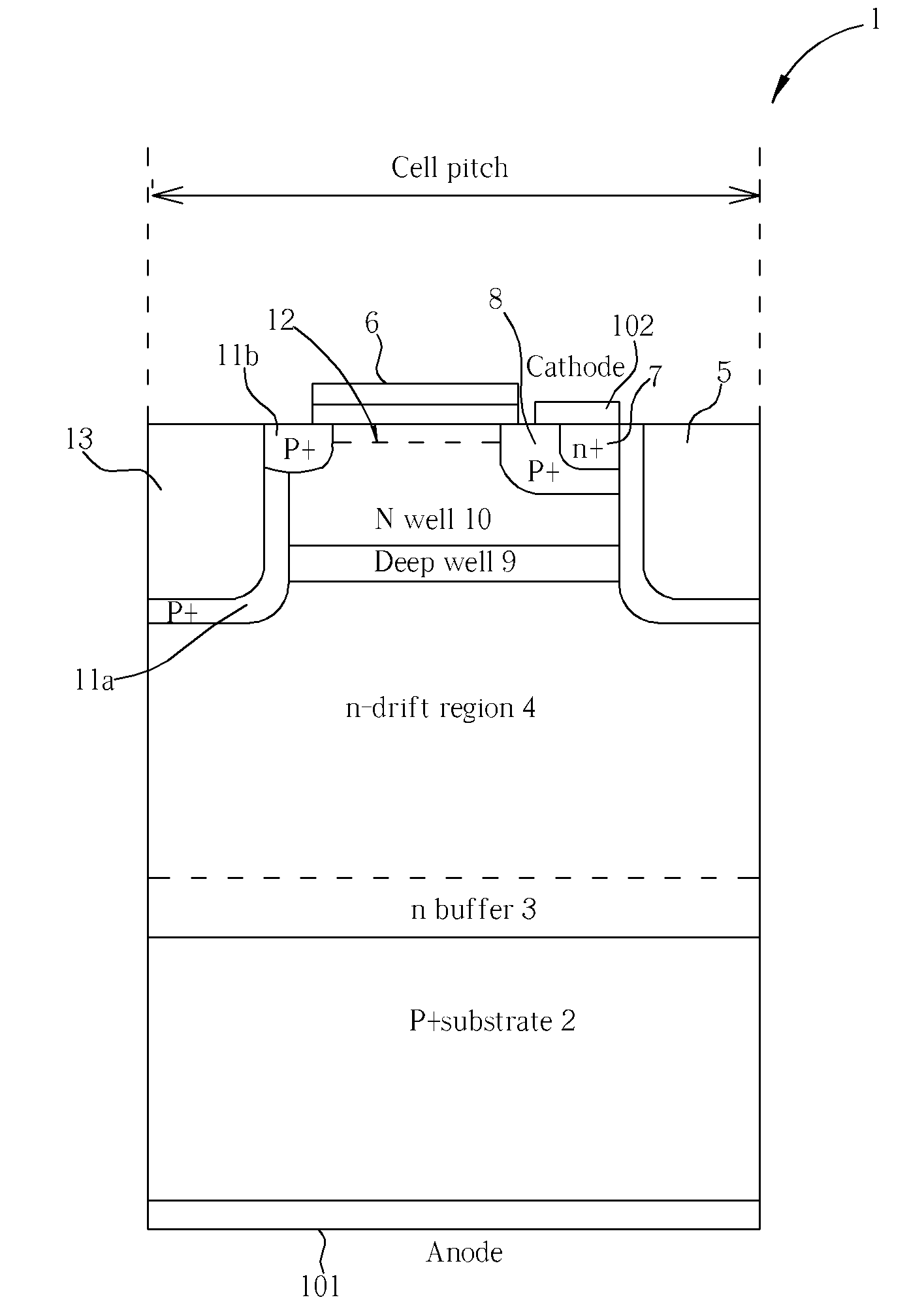
[0058]Referring to FIG. 5, an insulated gate bipolar transistor (IGBT) device 1 according to the present invention includes an anode terminal 101, a cathode terminal 102, a semiconductor substrate, 2, an n-type buffer layer 3 (optional), an n− drift region, 4, a first gate 5, a second gate 6, an n+ cathode region, 7, a p+ cathode short region 8, a deep p well 9, an n well 10, a p+ diffusion region 11b, a p+ layer 11 a disposed surrounding a metal plug 13, a pre-formed hole channel 12 at a surface of the n well 10 underneath the second gate 6, in which the first insulated gate 5 is a trench gate, the second (insulated) gate 6 is a planar gate adjacent to the cathode 102, and the first gate 5 and the second gate 6 are coupled together, and are referred to the cathode terminal 102.

second embodiment

[0059]Referring to FIG. 6, there is provided an insulated gate bipolar transistor (IGBT) device 1 according to the present invention comprising an anode terminal 101, a cathode terminal 102, a semiconductor substrate 2, an n-type buffer layer 3 (optional), an n− drift region 4, a first gate 5, a second gate 6, an n+ cathode region 7, a p+ cathode short region 8, a deep p well 9, an n well 10, a shallow p well 14, a pre-formed (buried) hole channel 12, in which the first gate 5 and the second gate 6 are a plurality of insulated trench gates which are coupled together, and are referred to the cathode 102; and the pre-formed hole channel 12 is disposed vertically along the trench wall of the second gate 6, and along a side surface of the n well 10, the shallow p well 14, and the deep p well 9.

[0060]Referring to FIG. 7, there is provided an equivalent circuit model of the device shown in FIG. 5 for the first embodiment, which includes a cathode, an anode, a first MOSFET 20b comprising a...

third embodiment

[0062]Referring to both FIGS. 7 & 8, there is provided an IGBT device according to the present invention where upon an application of a common 0V to the first gate and the second gate (or a voltage greater than zero volts but lower than the threshold voltage of the second MOSFET), the first MOSFET 20b is turned OFF and the second MOSFET 25a is turned ON, thereby allowing access for hole draining from the p type base layer, the deep p well, during the turn-off mode, and the potential of the p-base is clamped to that of the cathode during the off-state mode.

[0063]Referring to both FIGS. 5 & 6, there is provided an IGBT device according to the first and second embodiments, further including a first bipolar pnp transistor 30a, which is formed using the deep p well 9 as the emitter, the n well 10 as the base, and the p+ cathode 8 as the collector layer. The gain of the first bipolar pnp transistor 30a is controlled by controlling the thickness and doping of the base of the first bipolar ...


PUM


Abstract

Double gate IGBT having both gates referred to a cathode in which a second gate is for controlling flow of hole current. In on-state, hole current can be largely suppressed. While during switching, hole current is allowed to flow through a second channel. Incorporating a depletion-mode p-channel MOSFET having a pre-formed hole channel that is turned ON when 0V or positive voltages below a specified threshold voltage are applied between second gate and cathode, negative voltages to the gate of p-channel are not used. Providing active control of holes amount that is collected in on-state by lowering base transport factor through increasing doping and width of n well or by reducing injection efficiency through decreasing doping of deep p well. Device includes at least anode, cathode, semiconductor substrate, n− drift region, first & second gates, n+ cathode region; p+ cathode short, deep p well, n well, and pre-formed hole channel.

Description

CROSS REFERENCE TO RELATED APPLICATIONS[0001]This application claims the benefit of U.S. Provisional Application No. 60 / 947,992, filed Jul. 05, 2007.BACKGROUND OF THE INVENTION[0002]1. Field of the Invention[0003]This invention relates to an insulated gate bipolar transistor, and in particular, to a double gate insulated gate bipolar transistor (DG IGBT), and a method of manufacturing thereof.[0004]2. Description of the Prior Art[0005]An insulated gate bipolar transistor (IGBT) features a MOS gate for high impedance voltage-control and bipolar conduction for reducing the drift on-state resistance (through ‘conductivity modulation’). It can be seen as a successful combination between a power MOSFET and a bipolar transistor.[0006]Various versions of IGBTs have been developed. One is a trench IGBT (FIG. 1), which is a variant of an IGBT featuring a plurality of vertical channels 50a. Referring to FIG. 1, the trench IGBT device features an n− drift region where the voltage is supported ...

Claims


Application Information

Patent Timeline
Patent Type & Authority Applications(United States)
IPC IPC(8): H01L29/745H01L21/331
CPCH01L29/0696H01L29/4232H01L29/7397H01L29/7396H01L29/66348
Inventor UDREA, FLORIN
Owner ANPEC ELECTRONICS CORPORATION
Why Eureka
Try Eureka