Body-contacted finfet

Active Publication Date: 2009-01-08
GLOBALFOUNDRIES US INC
View PDF27 Cites 195 Cited by
  • Summary
  • Abstract
  • Description
  • Claims
  • Application Information

AI Technical Summary

Problems solved by technology

However, finFETs fabricated on a SOI substrate suffer from floating body effects, as is well known for conventional planar MOSFETs.
As such, floating body finFETs experience threshold voltages which are difficult to anticipate and control, and which vary in time.
The body charge storage effects result in dynamic sub-threshold voltage (sub-Vt) leakage and threshold voltage (Vt) mismatch among geometrically identical adjacent devices.
The floating body also poses leakage problems for pass gate devi

Method used


Image

  • Body-contacted finfet
  • Body-contacted finfet
  • Body-contacted finfet

Examples


embodiment # 1

Embodiment #1

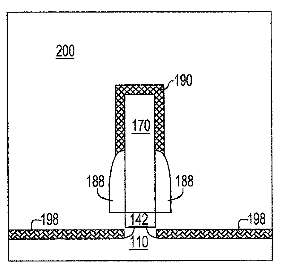
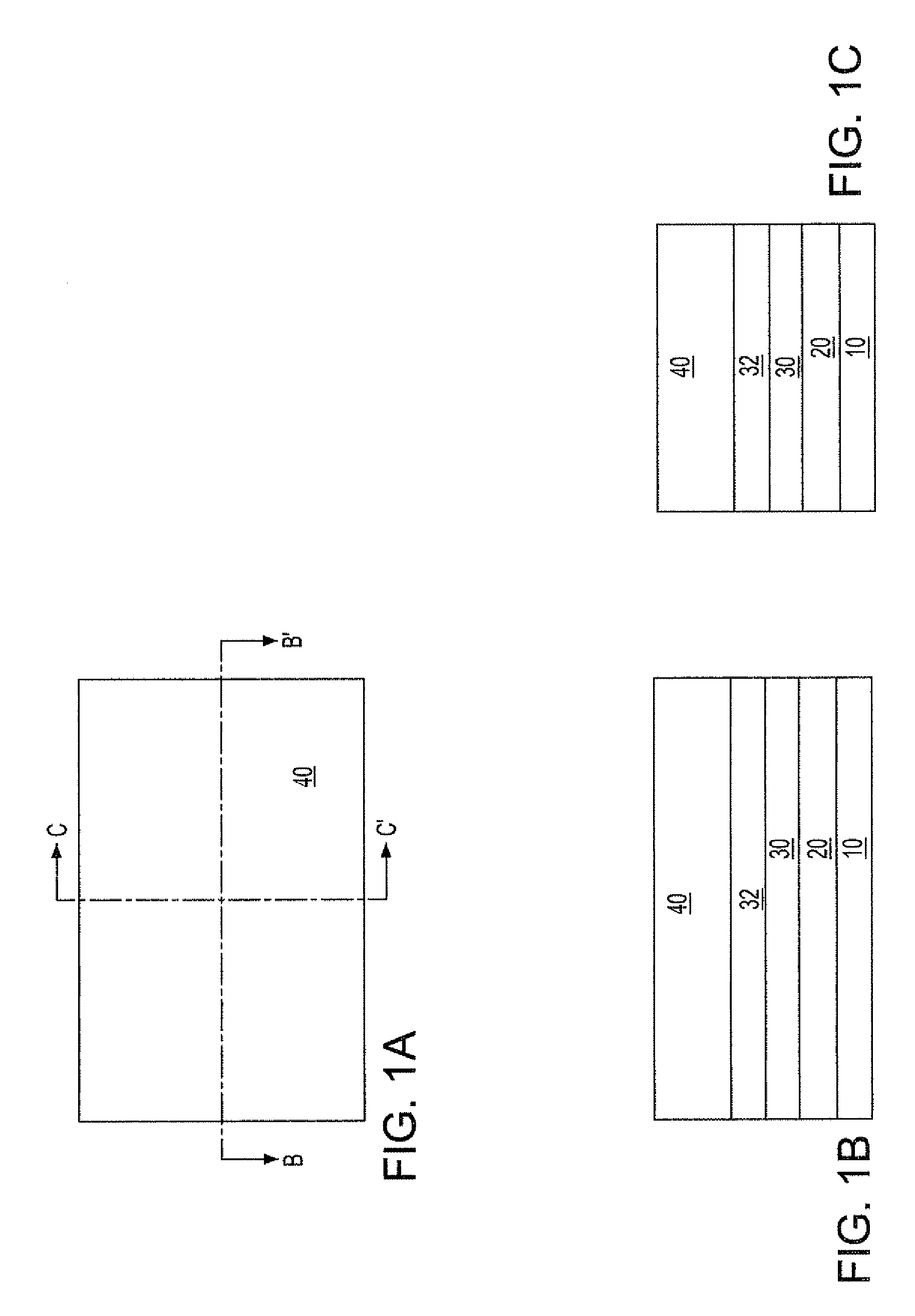
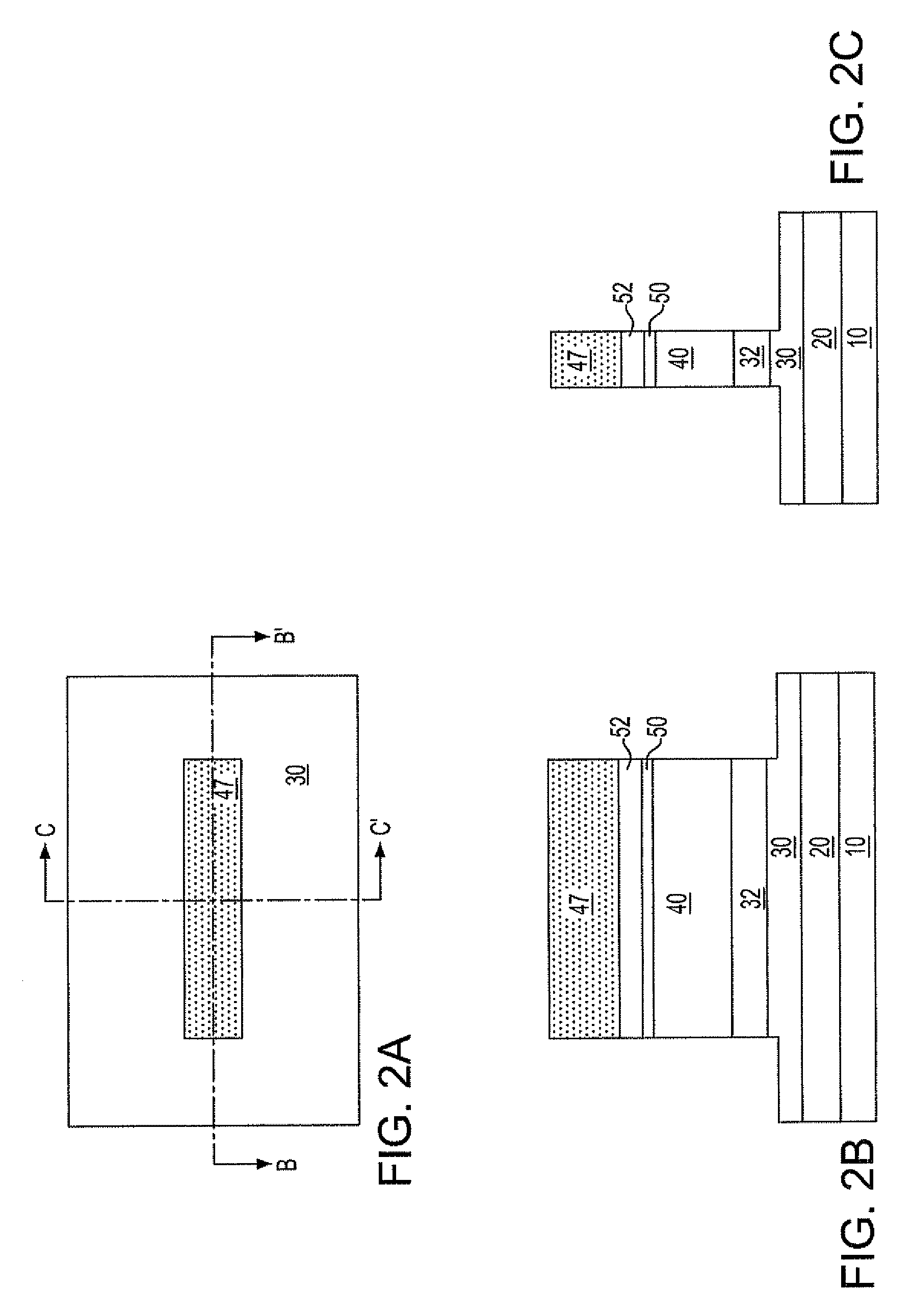
[0048]Referring to FIGS. 1A-1C, a first exemplary semiconductor structure according to a first embodiment of the present invention comprises a semiconductor-on-insulator (SOI) substrate having a handle substrate 10, a buried insulator layer 20, a first top semiconductor layer 30, a second semiconductor layer 32, and a third semiconductor layer 40. The three top semiconductor layers (30, 32, 40) are single crystalline and epitaxially aligned among one another.

[0049]The second top semiconductor layer 32 comprises a silicon germanium alloy with an atomic concentration of germanium from about 2 percent to about 15 percent, and preferably from about 2 percent to about 5 percent. The third top semiconductor layer 40 may comprise silicon and have inconsequential amount of germanium, for example, less than 0.1 percent. The third top semiconductor layer 40 may consist of silicon and electrical dopants such as B, Ga, In, P, As, and / or Sb. The second top semiconductor layer 32 may...

embodiment # 2

Embodiment #2

[0075]Referring to FIGS. 15A-15C, a second exemplary semiconductor structure according to a second embodiment of the present invention is shown, which comprises a fin cap dielectric layer 151 formed on a top surface of an initial semiconductor substrate 109. The initial semiconductor substrate 109 may comprise any semiconductor material including, but not limited to: Si, SiC, SiGe, SiGeC, Ge alloys, GaAs, InAs, InP, other III-V or II-VI compound semiconductors. It is preferred that the initial semiconductor substrate 109 be composed of a Si-containing semiconductor material, i.e., a semiconductor material that includes silicon. The initial semiconductor substrate 109 may be p-doped or n-doped with a dopant concentration typically from about 5.0×10¹⁵ / cm3 to about 3.0×10¹⁷ / cm3. The doping type of the initial semiconductor substrate 109 is herein referred to as a first conductivity type.

[0076]The fin cap dielectric layer 151 may comprise a nitride, an oxide, or a stack the...


PUM


Abstract

A silicon containing fin is formed on a semiconductor substrate. A silicon oxide layer is formed around the bottom of the silicon containing fin. A gate dielectric is formed on the silicon containing fin followed by formation of a gate electrode. While protecting the portion of the semiconductor fin around the channel, a bottom portion of the silicon containing semiconductor fin is etched by a isotropic etch leaving a body strap between the channel of a finFET on the silicon containing fin and an underlying semiconductor layer underneath the silicon oxide layer. The fin may comprise a stack of inhomogeneous layers in which a bottom layer is etched selectively to a top semiconductor layer. Alternatively, the fin may comprise a homogeneous semiconductor material and the silicon containing fin may be protected by dielectric films on the sidewalls and top surfaces of the silicon containing fin.

Description

FIELD OF THE INVENTION[0001]The present invention relates to semiconductor devices, and particularly to finFET structures with a body contact and methods of manufacturing the same.BACKGROUND OF THE INVENTION[0002]Fin metal-oxide-semiconductor field effect transistor (FinMOSFET) is an emerging technology which provides solutions to metal-oxide-semiconductor field effect transistor (MOSFET) scaling problems at, and below, the 45 nm node. FinMOSFET structures include fin field effect transistors (finFETs), which comprise at least one narrow (preferably <10 nm wide) semiconductor fin gated on at least two opposing sides of each of the at least one semiconductor fin. Preferred prior art finFET structures are formed on a semiconductor-on-insulator (SOI) substrate, because of low source / drain diffusion to substrate capacitance and ease of electrical isolation by shallow trench isolation structures.[0003]However, finFETs fabricated on a SOI substrate suffer from floating body effects, as...

Claims


Application Information

Patent Timeline
IPC IPC(8): H01L29/78H01L21/336
CPCH01L29/66795H01L29/785H01L29/7842
Inventor ZHU, HUILONGDYER, THOMAS W.MANDELMAN, JACK A.RAUSCH, WERNER
Owner GLOBALFOUNDRIES US INC
Why Eureka
Try Eureka