Antenna Array Feed Line Structures For Millimeter Wave Applications

a technology of antenna array and feed line structure, applied in the direction of resonant antenna, particular array feeding system, radiating element structure, etc., can solve the problems of microstrip feed line network use, difficult to obtain desired gain characteristics, and certain amount of loss of antenna efficiency and gain, etc., to achieve high-efficiency operation

Active Publication Date: 2009-01-08
GLOBALFOUNDRIES US INC
View PDF3 Cites 92 Cited by
  • Summary
  • Abstract
  • Description
  • Claims
  • Application Information

AI Technical Summary

Benefits of technology

[0010]In general, exemplary embodiments of the invention include improved feed line networks for antenna arrays operating at millimeter wave frequencies. In particular, exemplary embodiment of the invention include methods for constructing planar antenna arrays printed on the surface of a dielectric substrate wherein the planar antenna arrays are designed with an array of planar radiator elements interconnected through a feed line network of planar coplanar transmission lines which enable high-efficiency operation at millimeter wave operating frequencies. For example, an antenna array comprising an array of antenna radiator elements and feed network that is coplanar with the antenna elements can be formed with the feed network comprising coplanar strip line transmission lines including one or more coplanar strip line (CPS) and one or more coplanar waveguide (CPW) transmission line, which are interconnected using balun structures.

Problems solved by technology

As the size of the antenna array increases (and size of microstrip network) or as the operating frequency increases, the use of microstrip feed line networks are problematic.
However, as the number of patches used in a microstrip antenna array increases, it may be difficult to obtain the desired gain characteristics dues to large feeding losses that result from the antenna feed network.
Indeed, a corporate microstrip feed network, like any feed network, will result in a certain amount of loss of antenna efficiency and gain, due to losses in the microstrip lines, undesired radiation from, the lines, and mutual coupling between patches via surface waves.
Moreover, it is well known that a microstrip antenna structure having a microstrip feed network and patch array on the same level (on the same substrate surface) cannot be optimized simultaneously because the requirements for microstrip antennas and microstrip transmission lines are different.
However, lower dielectric constant substrates and thicker substrates can result in spurious radiation from microstrip line and step discontinuities.
However, for applications at millimeter wave operating frequencies and beyond, microstrip patch antenna arrays cannot be easily implemented on a substrate as thin as 100 um or thinner due to mechanical reliability and limitations of the manufacturing process, as is understood by those of ordinary skill in the art.
As a result the substrate is usually too thick for microstrip lines operating at mmWave and higher frequencies.
Under these conditions, the microstrip line does not properly operate as a feed line, but operates as a radiating element as well.
Therefore, for millimeter wave frequencies and beyond, it is virtually impossible to design efficient planar antenna arrays with coplanar microstrip lines, even for small arrays with, e.g., four elements.

Method used


Image

  • Antenna Array Feed Line Structures For Millimeter Wave Applications
  • Antenna Array Feed Line Structures For Millimeter Wave Applications
  • Antenna Array Feed Line Structures For Millimeter Wave Applications

Examples


Embodiment Construction

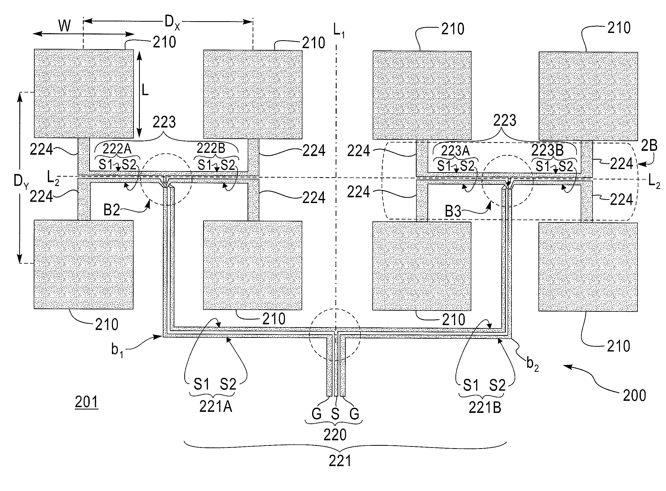
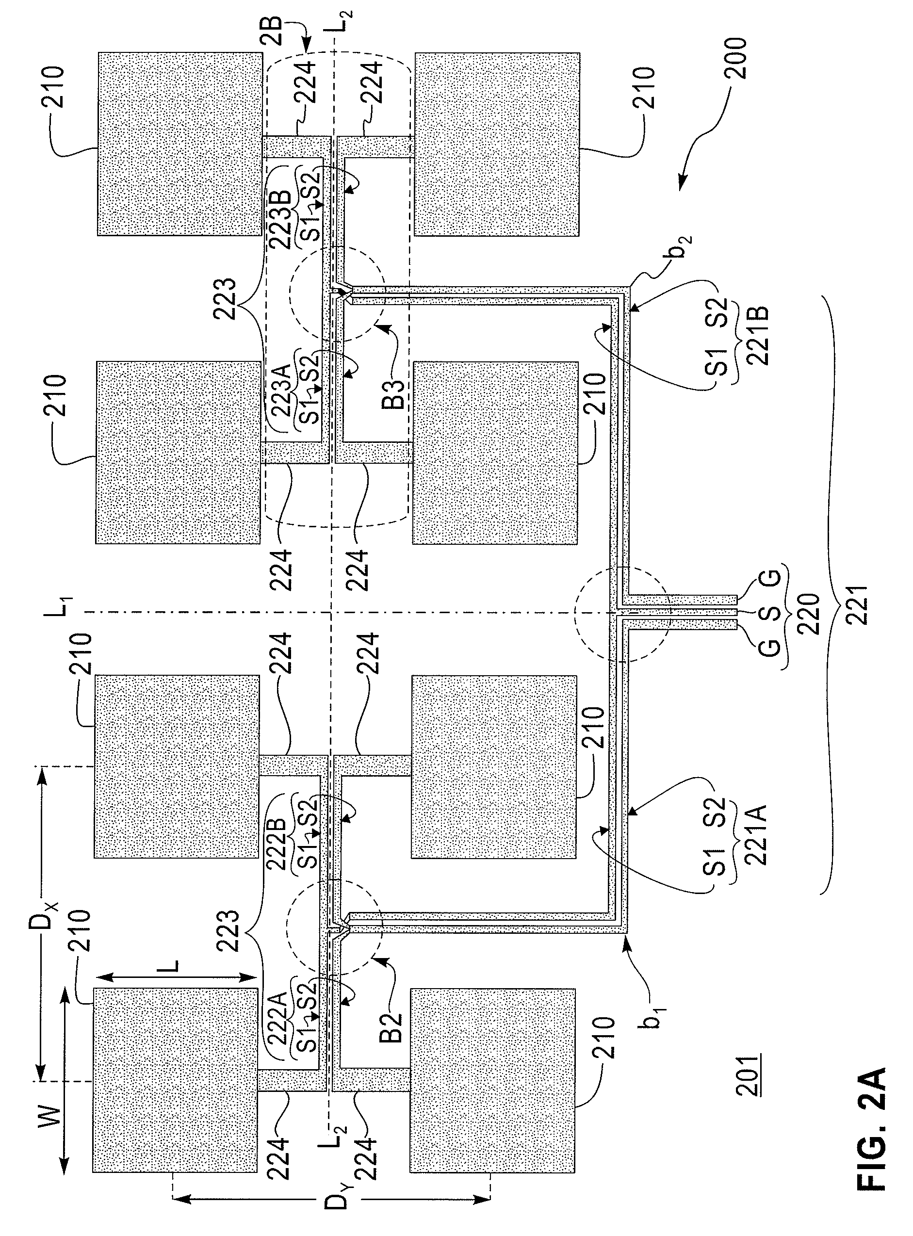
[0022]FIGS. 2A˜2B are schematic views of an antenna array device comprising an array of planar radiating elements interconnected by a feed network of coplanar transmission lines, according to an exemplary embodiment of the invention. In general, FIG. 2A is a schematic plan view of an antenna array device comprising a planar antenna array (200) that is patterned or otherwise formed on one side of a dielectric substrate (201). FIG. 23 is a detailed plan view of the portion of the planar antenna array (200) within the dashed region 2B shown in FIG. 2A. In general, the planar antenna array (200) comprises an array of radiating patch elements (210) that are uniformly arranged in rows and columns (2×4) of patch elements (210). The array of patch elements (210) are fed by a corporate structured feed network comprising coplanar transmission lines (220, 221, 222, 223), and short microstrip lines (224) that directly connect to feed points at edges of the patch elements (210). In the exemplary...


PUM


Abstract

Improved feed line networks for antenna arrays operating at millimeter wave frequencies are provided for constructing planar antenna arrays printed on the surface of a dielectric substrate. A planar antenna array includes an array of planar radiator elements interconnected through a feed line network of planar coplanar transmission lines that enable high-efficiency operation, at millimeter wave operating frequencies. For example, a feed network may be formed with a network of coplanar strip line transmission lines including one or more coplanar strip line (CPS) and one or more coplanar waveguide (CPW) transmission line, which are interconnected using balun structures, to enable high efficiency operation at millimeter wave frequencies.

Description

GOVERNMENT LICENSE RIGHTS[0001]This invention was made with Government support under Contract No. N66001-02-C-8014 and N66001-05-C-8013 awarded by DARPA (Defense Advanced Research Projects Agency). The Government has certain rights in this invention.TECHNICAL FIELD OF THE INVENTION[0002]The present invention generally relates to improved feed line networks for antenna arrays operating at millimeter wave frequencies and, in particular, a planar antenna array printed on the surface of a dielectric substrate wherein the planar antenna array includes an array of planar radiator elements interconnected through a feed line network of planar coplanar transmission lines to provide high-efficiency operation at millimeter wave operating frequencies.BACKGROUND[0003]In the wireless communications industry, market demands for ubiquitous network access to information and services has been met with rapid and widespread development of wireless network applications for wireless PAN (personal area ne...

Claims


Application Information

Patent Timeline
Patent Type & Authority Applications(United States)
IPC IPC(8): H01Q9/04
CPCH01Q21/0006H01Q21/065H01Q21/062H01Q21/0075
Inventor GAUCHER, BRIAN PAULLIU, DUIXIANSIRDESHMUKH, RANJANI
Owner GLOBALFOUNDRIES US INC
Why Eureka
Try Eureka