Electrical fuse having a cavity thereupon

a technology of electrical fuse and cavity, applied in the direction of transistors, semiconductor/solid-state device details, instruments, etc., can solve the problems of adverse effects on the performance of many semiconductor devices, and achieve the effects of less programming current, enhanced thermal isolation of electrical fuse, and superior thermal isolation

Inactive Publication Date: 2009-01-22
IBM CORP
View PDF4 Cites 28 Cited by
  • Summary
  • Abstract
  • Description
  • Claims
  • Application Information

AI Technical Summary

Benefits of technology

[0010]An electrical fuse is formed on a semiconductor substrate and a first dielectric layer is formed over the electrical fuse. At least one opening is formed by lithographic methods and a reactive ion etch in the first dielectric layer down to a top surface of the electrical fuse or down to shallow trench isolation. The at least one opening has at least one lateral dimension that is less than one half, and preferably less than one third, of the height of the first dielectric layer. A second dielectric layer is deposited by a non-conformal deposition. Thickness of the second dielectric layer on the sidewalls of the at least one opening increases with height so that at least one cavity encapsulated by the second dielectric layer is formed in the at least one opening. The at least one cavity provides enhanced thermal isolation of the electrical fuse since the cavity provides superior thermal isolation than a dielectric material. The electrical fuse may be programmed with less programming current and semiconductor devices nearby are protected from adverse thermal effects during programming.

Problems solved by technology

Further, performance of many semiconductor devices may be adversely impacted by a high temperature, for example, through diffusion of dopants or decomposition of a thermally susceptible material.

Method used


Image

  • Electrical fuse having a cavity thereupon
  • Electrical fuse having a cavity thereupon
  • Electrical fuse having a cavity thereupon

Examples


first embodiment

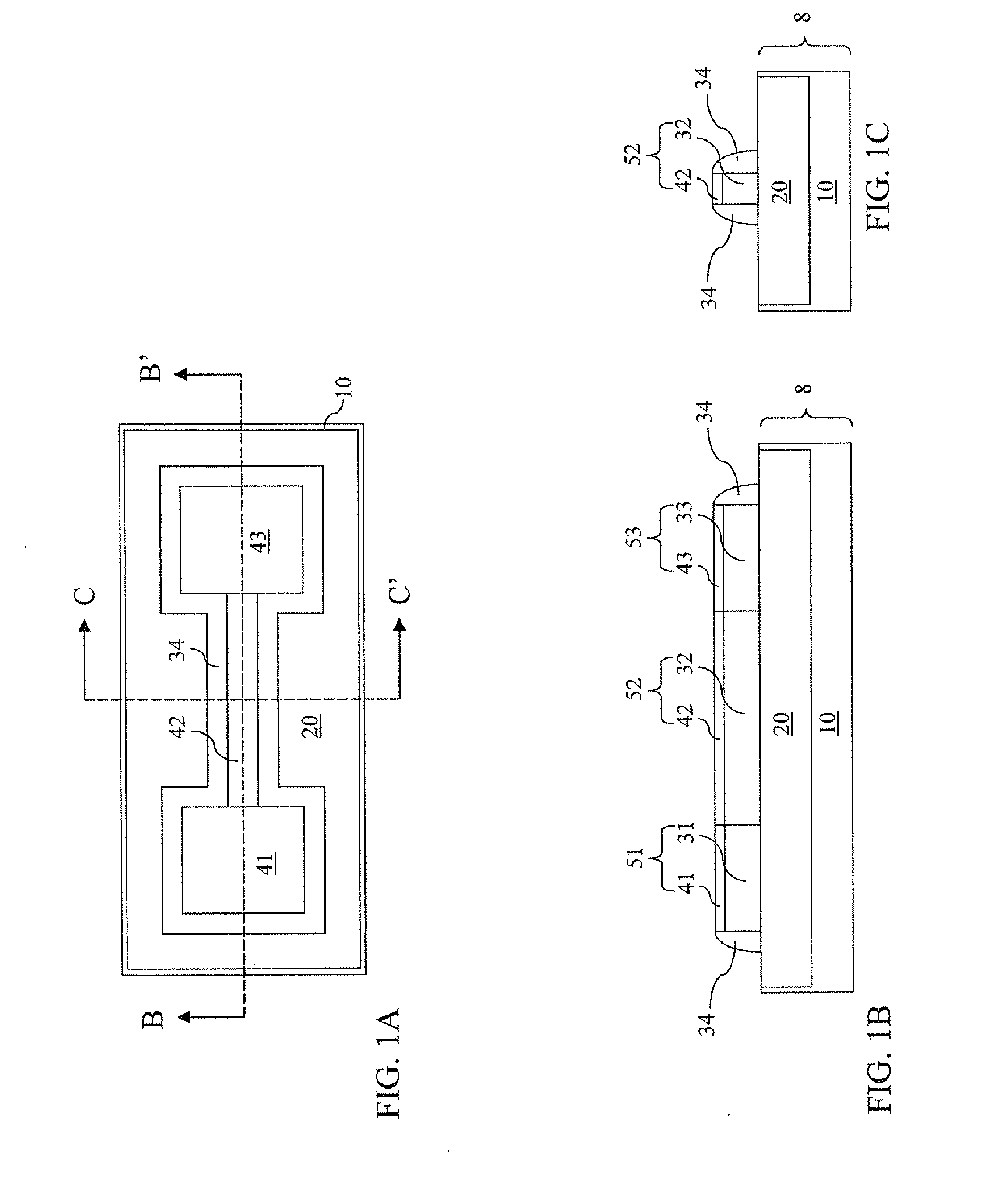
[0070]An optional dielectric cap layer 40 may be deposited on the first dielectric layer 40. The thickness of the optional dielectric cap layer 40 may be from about 5 nm to about 200 nm, and typically from about 20 nm to about 50 nm. The optional dielectric cap layer 40 may comprise a silicon oxide, a silicon nitride, or a stack thereof. In a variation of the first embodiment, the optional dielectric cap layer is omitted so that the photoresist 41 is applied directly on the first dielectric layer 36.

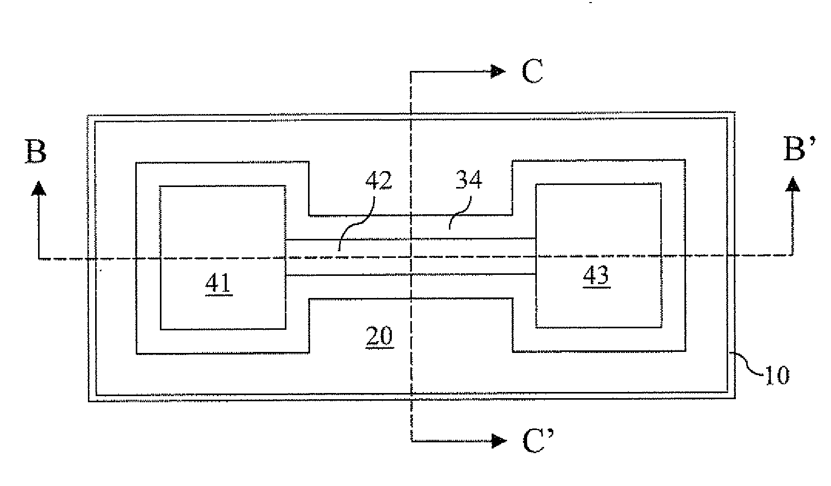
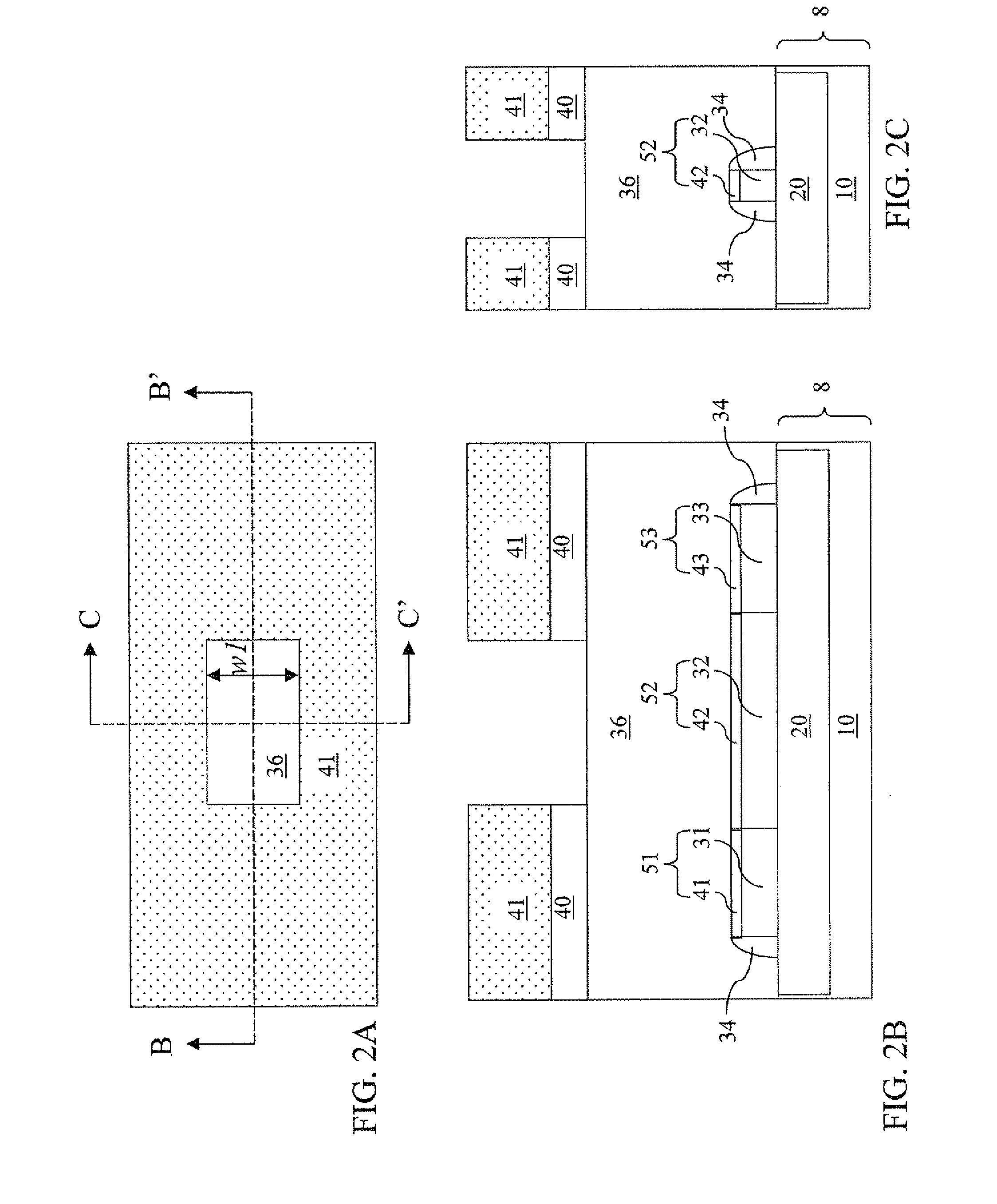
[0071]A photoresist 41 is applied on the optional dielectric cap layer 40 and lithographically patterned to expose a portion of the optional dielectric cap layer 40 over the fuselink 52. An opening having a lithographic dimension is patterned in the photoresist 41. The opening may be rectangular and may have a first lithographic width w1 in the direction perpendicular to the direction between the first electrode 51 and the second electrode 53. The first lithographic width w1 may be great...

second embodiment

[0086]A second exemplary structure according to the present invention is derived from the first exemplary structure shown in FIGS. 2A-2C by reducing the first lithographic width w1. Specifically, the opening formed in the photoresist 41 (See FIGS. 2A-2C) has a second lithographic width w2 in the direction perpendicular to the direction between the first electrode 51 and the second electrode 53. The second lithographic width w2 is a lithographic dimension, i.e., is equal to or greater than the lithographic minimum dimension. The second lithographic dimension w2 is less than the sum of the width of the fuselink 52 and twice the width of the dielectric spacer 34.

[0087]Referring to FIGS. 7A-7C, the optional dielectric cap layer 40 and the first dielectric layer 36 are etched to form an opening in the first dielectric layer 36 as in the first embodiment. A top surface of the fuselink 52 and a top surface of portions of the dielectric spacer 34 are exposed within the opening in the first ...

fourth embodiment

[0096]Referring to FIGS. 13 A-13C, a fifth exemplary semiconductor structure is formed by etching at least one additional volume of the first dielectric layer 36 connecting portion of the opening in the first dielectric layer 36 around the periphery of the electrical fuse (51, 52, 53) of the fourth exemplary structure in FIGS. 11A-11C. The cavity encircles a first portion of the first dielectric layer 36 located above the first electrode 51, a second portion of the first dielectric layer 36 located above the second electrode 52, and a third portion of the first dielectric layer 36 located above the fuselink 52. The opening in the first dielectric layer 36 comprises multiple trenches that are interconnected. The opening may have substantially the same width, which is the fourth lithographic dimension w4, or may have a local variation. The width of the opening, i.e., the lateral dimension between two opposing sidewalls of the first dielectric layer in the opening, is lithographic as i...


PUM


Abstract

An electrical fuse is formed on a semiconductor substrate and a first dielectric layer is formed over the electrical fuse. At least one opening is formed by lithographic methods and a reactive ion etch in the first dielectric layer down to a top surface of the electrical fuse or down to shallow trench isolation. A second dielectric layer is deposited by a non-conformal deposition. Thickness of the second dielectric layer on the sidewalls of the at least one opening increases with height so that at least one cavity encapsulated by the second dielectric layer is formed in the at least one opening. The at least one cavity provides enhanced thermal isolation of the electrical fuse since the cavity provides superior thermal isolation than a dielectric material.

Description

FIELD OF THE INVENTION[0001]The present invention relates to semiconductor structures, and particularly to an electrical fuse having at least one cavity thereupon and methods of manufacturing the same.BACKGROUND OF THE INVENTION[0002]Electrical fuses (eFuses) are used in the semiconductor industry to implement array redundancy, field programmable arrays, analog component trimming circuits, and chip identification circuits. Once programmed, the programmed state of an electrical fuse does not revert to the original state on its own, that is, the programmed state of the fuse is not reversible. For this reason, electrical fuses are called One-Time-Programmable (OTP) memory elements.[0003]The mechanism for programming an electrical fuse is electromigration of a metal semiconductor alloy induced by an applied electrical field and an elevated temperature on a portion of the electrical fuse structure. The metal semiconductor alloy is electromigrated under these conditions from the portion o...

Claims


Application Information

Patent Timeline
Patent Type & Authority Applications(United States)
IPC IPC(8): H01H85/165
CPCG11C17/16H01L21/76229H01L2924/12044H01L27/112H01L27/11206H01L23/5256H01L2924/0002H10B20/00H10B20/20H01L2924/00
Inventor KIM, DEOK-KEELI, WAI-KINYANG, HAINING S.
Owner IBM CORP
Why Eureka
Try Eureka