Insulating Substrate and Manufacturing Method Therefor, and Multilayer Wiring Board and Manufacturing Method Therefor

a technology of insulation substrate and manufacturing method, which is applied in the direction of printed circuit, thin material processing, electrical equipment, etc., can solve the problems of method paying attention, multi-layer wiring boards of related art, and inability to meet such a demand, so as to reduce shrinkage variations.

Inactive Publication Date: 2009-01-29
KYOCERA CORP
View PDF22 Cites 6 Cited by
  • Summary
  • Abstract
  • Description
  • Claims
  • Application Information

AI Technical Summary

Benefits of technology

[0014]Accordingly, it is an object of the invention to provide a dimensionally accurate insulating substrate in which plane direction-wise shrinkage is reduced to practically zero and shrinkage variations can be decreased, as well as to provide a method for manufacturing the insulating substrate.
[0015]It is another object of the invention to provide a dimensionally accurate multilayer wiring board having excellent electrical characteristics that is fabricated by firing together a plurality of stacked insulating layers that exhibit different firing shrinkage curves (shrinking behaviors) in a manner so as to insure that the insulating layers of different types are inhibited from shrinking in a plane direction by each other, as well as to provide a method for manufacturing the multilayer wiring board.
[0016]It is yet another object of the invention to provide a multilayer wiring board that is small in thickness and nevertheless suffer little from warpage.

Problems solved by technology

Unfortunately, multilayer wiring boards of a related art, however, failed to meet such a demand.
However, these methods have encountered the following problems.
Namely, the former adopting the pressure-firing technique necessitates not only a warpage-free Al2O3 sintered plate but also specially-devised pressurizing means, whereas the latter exploiting the arresting action of the unfired ceramic layer (restrictive firing) necessitates a step for removing the unfired ceramic layer after the firing process is over, which is liable to result in an undesirable increase in the number of manufacturing process steps.
However, on the negative side, this method pays heed only to the control of firing shrinking starting temperatures.
This could give rise to problems such as occurrence of appreciable shrinking-behavior variations under restriction and a failure of ensuring sufficiently low shrinkage.
However, only with this advantage, it is difficult to ensure that the plane direction-wise shrinkage of the substrate becomes practically zero, or undesirable shrinkage variations are inevitable.
This imposes limitations on material design and thus the characteristics of materials cannot be changed greatly.
As a result, asperities tend to appear at the interface between the wiring conductor layer and the insulating layer, in consequence whereof there results an increased conductor resistance and poor interface conductivity.
This leads up to electrical characteristic degradation in a resulting insulator layer with a built-in capacitor or the like function.
In the end, the ceramic molding and the conductor layer have been prone to vary in firing shrinking behavior, which leads up to appreciable warpage.

Method used


Image

  • Insulating Substrate and Manufacturing Method Therefor, and Multilayer Wiring Board and Manufacturing Method Therefor
  • Insulating Substrate and Manufacturing Method Therefor, and Multilayer Wiring Board and Manufacturing Method Therefor
  • Insulating Substrate and Manufacturing Method Therefor, and Multilayer Wiring Board and Manufacturing Method Therefor

Examples


first embodiment

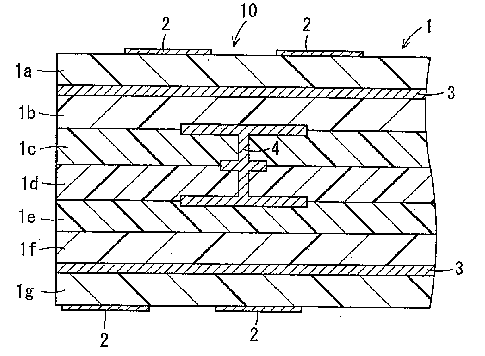
[0064]FIG. 1 is a schematic sectional view showing a multilayer wiring board according to a first embodiment of the invention. In FIG. 1, the multilayer wiring board 10 is composed of: an insulating substrate 1 composed of a laminated body constituted by stacking together insulating layers 1a through 1g; surface conductor layers 2 formed on the top and back surfaces of the insulating substrate 1; inner conductor layers 3 formed within the insulating substrate 1; and a via-hole conductor 4 for providing connection among the conductor layers.

[0065]In more detail, in the multilayer wiring board 10 of the invention having such a constitution, the insulating substrate 1 is formed by stacking a plurality of insulating layers 1a through 1g on top of one another thereby to assume a lamination structure. The inner conductor layer 3 is interposed between the adjacent insulating layers. The via-hole conductor 4 is so formed as to extend penetratingly through at least one of the insulating laye...

second embodiment

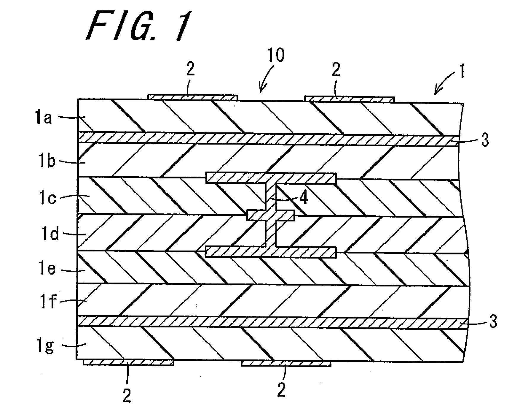
[0102]FIG. 2 is a schematic sectional view showing a multilayer wiring board according to a second embodiment of the invention. In FIG. 2, the multilayer wiring board 2 is composed of: an insulating substrate 11 constituted by stacking together second insulating sheets 11a through 11c which are ceramic green sheets and combined layers 12a and 12b; surface conductor layers 12 formed on the top and back surfaces of the insulating substrate 11; inner conductor layers 13 formed within the insulating substrate 11; and a via-hole conductor 14 for providing connection among the conductor layers.

[0103]The combined layers for constituting the insulating substrate 11 are composed of first and second insulating sheets which are ceramic green sheets having different shrinking starting temperatures. Specifically, the firing shrinking starting temperature of the insulating sheets 12a-(1) 12b-(1) is lower than those of the other insulating sheets 12a-(2), 12b-(2), and 11a through 11c. Meanwhile, t...

example 1

[0128]Referring to Table 1, glass powder and ceramic powder serving as filler were mixed together at the mixing ratio shown in Table 1. Then, ethylcellulose (organic binder) and 2-2-4 trimethyl pentadiol monoisobutyrate (organic solvent) are blended into the powder admixture to form a slurry. The slurry was molded into a thin-layer component by the doctor blade method to obtain green sheets. Whereupon, the insulating sheets for constituting a multilayer insulating substrate were prepared for use (sheets A through H). Note that the crystallization temperature Tc of the glass and the softening point Tg of the glass were determined, by means of DTA (Differential Thermal Analysis), in accordance with a curve obtained with a temperature rising speed kept at 10° C. / min.

[0129]Also listed in Table 1 are the firing shrinking starting temperatures, shrinking ending temperatures, thermal expansion coefficients, and dielectric constants of the individual insulating sheets. In carrying out data ...


PUM

PropertyMeasurementUnit
sheet resistanceaaaaaaaaaa
softening pointaaaaaaaaaa
temperatureaaaaaaaaaa

Abstract

There is provided a dimensionally accurate insulating substrate in which plane direction-wise shrinkage is practically zero and shrinkage variations are small. The insulating substrate includes a laminated body composed of at least two kinds of insulating layers made of crystallizable glass ceramics. The crystallization temperature of crystallizable glass contained in the first insulating layer is lower than the softening point of crystallizable glass contained in the second insulating layer. The difference in thermal expansion coefficient between the first and second insulating layers is preferably 2×10⁻⁶ / ° C. or below.

Description

BACKGROUND OF THE INVENTION[0001]1. Field of the Invention[0002]The present invention relates to an insulating substrate, which is suitable for use as a circuit board, and a manufacturing method for the insulating substrate, and a multilayer wiring board and a manufacturing method for the multilayer wiring board.[0003]2. Description of the Related Art[0004]While multilayer wiring boards using ceramics as their insulating substrates have conventionally been in wide use, in keeping with the recent demand for multilayer wiring boards provided with various functions, multilayer wiring boards fabricated by the use of a combination of ceramics materials of different types have been proposed to date. For example, there are known a multilayer wiring board that offers high strength by using a combination of a low-strength ceramic insulating layer and a high-strength ceramic insulating layer, and a multilayer wiring board that allows incorporation of a high-capacitance capacitor by using a la...

Claims


Application Information

Patent Timeline
Patent Type & Authority Applications(United States)
IPC IPC(8): C03B32/02
CPCB32B18/00Y10T428/24926B32B2307/734C03C10/0045C03C10/0054C03C14/004C04B35/117C04B35/6365C04B37/04C04B2235/3206C04B2235/3481C04B2235/365C04B2235/6025C04B2235/80C04B2235/9607C04B2235/9615C04B2237/62C04B2237/704H05K1/0306H05K3/4629H05K3/4688B32B2307/206
Inventor FURUSE, TATSUJIHIRAHARA, SEIICHIROYAMAMOTO, SENTAROUYAMAMOTO, KOUJIOGAWAUCHI, MITSUGIKAJIHARA, SATORU
Owner KYOCERA CORP
Why Eureka
Try Eureka