Plasma etching method, plasma etching apparatus and storage medium

a plasma etching and plasma technology, applied in the direction of electrical equipment, basic electric elements, electric discharge tubes, etc., can solve the problems of difficult to form finer holes, easy generation of cracks, surface state deterioration, etc., to reduce opening size, improve throughput, and increase the thickness of the photoresist film

Inactive Publication Date: 2009-01-29
TOKYO ELECTRON LTD
View PDF14 Cites 6 Cited by
  • Summary
  • Abstract
  • Description
  • Claims
  • Application Information

AI Technical Summary

Benefits of technology

[0008]In view of the above, the present invention provides a plasma etching method and a plasma etching apparatus which are capable of performing etching while reducing an opening size of a photoresist pattern at a high etching rate and improving a surface state of a photoresist film by repairing cracks.
[0009]Further, the present invention provides a plasmas etching method and a plasma etching apparatus which are capable of etching an organic anti-reflection film with a high etching selectivity to a photoresist film.
[0013]The plasma etching method further includes, by the plasma, etching the etching target film through the opening formed in the photoresist film while reducing the opening size of the opening.
[0032]In accordance with the aspects of the present invention, a processing gas containing CF4 gas, CH2F2 gas, CxFy gas (x / y≧0.5) is used, and an etching target film is etched by using a plasma of the processing gas which is generated by applying a high frequency power to at least one of the first and the second electrode horizontally facing each other. Therefore, the effect of reducing an opening size by CF4 gas and CH2F2 gas is facilitated by using CxFy gas. Accordingly, an opening size decreasing rate is increased, thus improving a throughput. Moreover, the surface of the ArF photoresist film can be planarized by CxFy gas. In addition, the thickness of the photoresist film can be increased, and the cracks can be repaired. Accordingly, a single layer resist can be used instead of a multi layer resist that has been conventionally used to avoid an insufficient amount of the residual ArF photoresist film. Moreover, the present invention is especially suitable for a technique used for forming a pattern of a narrow width, such as a double patterning technique or the like.
[0033]In accordance with the present invention, a processing gas containing CF4 gas, CH2F2 gas, CxFy gas (x / y≧0.5) is used, and an etching target film is etched by using a plasma of the processing gas which is generated by applying a high frequency power to at least one of the first and the second electrode horizontally facing each other, as described above. In addition, by applying a DC voltage to any one of the first and the second electrode during the plasma generation, the polymers attached to the electrode to which the DC voltage is applied can be supplied to the target object. As a result, the above effects can be further enhanced.
[0035]In a target object manufactured by sequentially forming, on an etching target film, an organic antireflection film and a photoresist film thereon, when plasma etching is performed on the organic antireflection film and the etching target film by using the photoresist film as a mask, a processing gas containing CF4 gas, CH2F2 gas, CxFy gas (x / y≧0.5) is used, and an etching target film is etched by using a plasma of the processing gas which is generated by applying a high frequency power to at least one of the first and the second electrode horizontally facing each other. In addition, a DC voltage is applied to any one of the first and the second electrode during the plasma generation. At this time, the plasma generation time period is divided into a first and a second time period. In the first time period, the DC voltage is set to reduce the opening size of the opening. In the second time period, the DC voltage is set to etch the organic antireflection film with a selectivity higher than a predetermined value to the photoresist film. Accordingly, it is possible to improve a throughput by increasing an opening size decreasing rate, planarize a surface of an ArF photoresist film and etch an organic anti-reflection film with a high selectivity to a photoresist film.

Problems solved by technology

However, in a conventional photolithography process using an ArF photoresist, it is difficult to form a finer hole due to its limitation in miniaturization.
However, when the ArF photoresist is patterned by employing the photolithography, its surface state becomes deteriorated and, also, cracks are easily generated therein.
Accordingly, the amount of the residual ArF photoresist film is insufficient in the portions where the cracks are generated.
As a consequence, base wiring patterns are damaged, and this may lead to a short-circuit.
Besides, the technique of JP-A-2005-129893 is disadvantageous in that a long period of time is needed to reduce the opening size to a desired size, which deteriorates a throughput.
Accordingly, the amount of the residual mask film becomes insufficient.

Method used


Image

  • Plasma etching method, plasma etching apparatus and storage medium
  • Plasma etching method, plasma etching apparatus and storage medium
  • Plasma etching method, plasma etching apparatus and storage medium

Examples


first embodiment

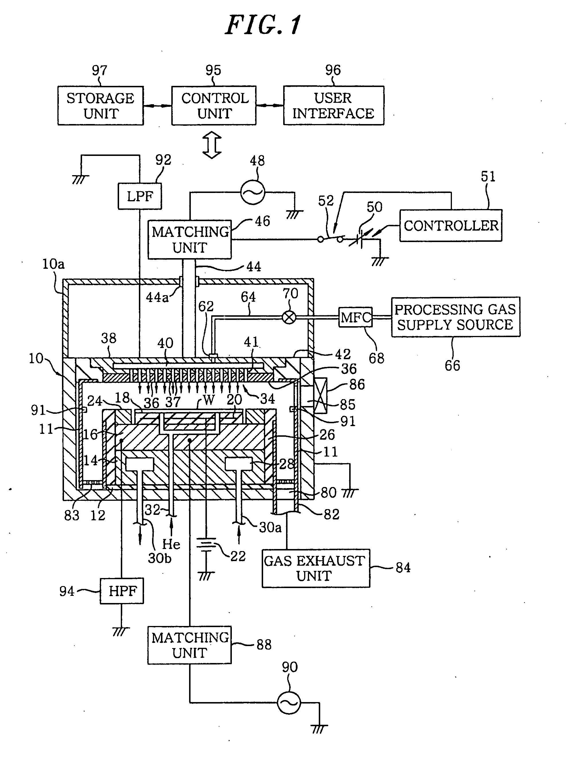
[0077]Hereinafter, there will be described a plasma etching method in accordance with the present invention, which is performed by the plasma etching apparatus having the aforementioned configuration.

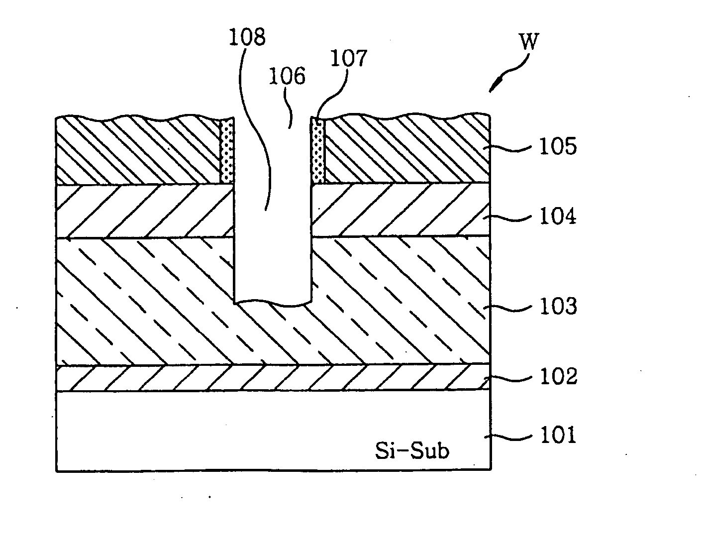
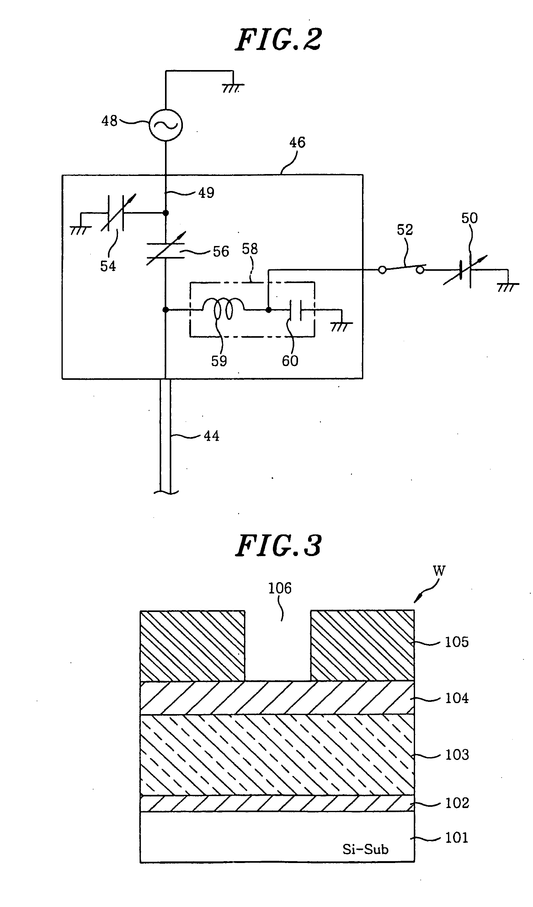
[0078]Here, a semiconductor wafer W to be processed has an etching stopper film 102, an etching target film 103, a bottom anti-reflection coating (BARC) film 104 and a patterned photoresist film 105 that are sequentially formed on a Si substrate 101 as shown in FIG. 3.

[0079]The etching stopper film 102 is, e.g., an SiC film. The etching target film 103 as an interlayer insulating film is, e.g., an SiO2 film or a Low-k film. The BARC film 104 is, e.g., an organic film, and its thickness is about 80 nm. The photoresist film 105 is, e.g., an ArF resist of which thickness is about 120 nm.

[0080]In a plasma etching processing, the gate valve 86 is first opened, and the semiconductor wafer W having the above-described configuration is loaded into the chamber 10 through the loading / unloading po...

second embodiment

[0114]Hereinafter, a plasma etching method in accordance with the present invention will be described.

[0115]In the second embodiment, a semiconductor wafer W shown in FIG. 10 is used as a substrate to be processed, the semiconductor having an etching stopper film 202, an etching target film 203, an organic BARC film 204 and a patterned photoresist film 205 which are sequentially formed on a Si substrate 201. Before etching the etching target film 203, the organic BARC film 204 is etched by using the photoresist film 205 as a mask.

[0116]When the etching is performed, the organic BARC film 204 needs to be etched with a high etching selectivity to the photoresist film 205 in view of ensuring a sufficient amount of a residual mask film. However, the organic BARC film 204 has a similar composition as that of the photoresist film 205 such as an ArF photoresist film or the like. Therefore, when the organic BARC film 204 is etched, the photoresist film 205 is etched at substantially the sam...


PUM

PropertyMeasurementUnit
DC voltageaaaaaaaaaa
frequencyaaaaaaaaaa

Abstract

A plasma etching method plasma-etches an etching target film by using a photoresist film as a mask. The plasma etching method includes loading a target object to be processed into a processing chamber where an upper and a lower electrode are provided to face each other, the target object having the etching target film and the photoresist film in which an opening is formed; introducing into the processing chamber a processing gas containing CF4 gas, CH2F2 gas and CxFy gas, wherein x / y≧0.5; and generating a plasma of the processing gas by applying a high frequency power to at least one of the upper and the lower electrode. The method further includes, by the plasma, etching the etching target film introduced through the opening formed in the photoresist film while reducing the opening size the opening.

Description

FIELD OF THE INVENTION[0001]The present invention relates to a method and an apparatus for performing plasma etching on a predetermined film of a target object, e.g., a semiconductor substrate and the like, by using as a mask a photoresist film, e.g., an ArF resist film or the like, and a storage medium storing a program for executing the plasma etching method.BACKGROUND OF THE INVENTION[0002]In a semiconductor device manufacturing process, a photolithography process is performed to form a photoresist pattern on a semiconductor wafer as a target object, and an etching process is performed by using the photoresist pattern as a mask.[0003]To match a recent progress in miniaturization of semiconductor devices, it becomes necessary to employ microprocessing in etching. To this end, in micro-etching, a thickness of a photoresist film used as a mask is getting thinner, and an ArF photoresist (i.e., a photoresist exposed to a laser beam having a shorter wavelength of which an emission sour...

Claims


Application Information

Patent Timeline
Patent Type & Authority Applications(United States)
IPC IPC(8): H01L21/302
CPCH01J37/32091H01J37/32174H01J37/32697H01L21/31144H01L21/31116H01L21/31138H01J2237/334H01L21/3065
Inventor KIKUCHI, AKIHIROIDEHARA, KENJI
Owner TOKYO ELECTRON LTD
Why Eureka
Try Eureka