Asymmetric bidirectional silicon-controlled rectifier

a silicon-controlled rectifier, bi-directional technology, applied in the direction of diodes, semiconductor devices, electrical apparatus, etc., can solve the problems of easy damage to the thin gate oxide layer of the submicron or deep submicron technology, easy damage to the integrated circuit product, and low esd robustness, so as to prevent electrostatic charge

Active Publication Date: 2009-02-05
AMAZING MICROELECTRONICS
View PDF8 Cites 32 Cited by
  • Summary
  • Abstract
  • Description
  • Claims
  • Application Information

AI Technical Summary

Benefits of technology

[0008]The primary objective of the present invention is to provide an asymmetric bidirectional silicon-controlled rectifier, which can prevent electrostatic charge from damaging a semiconductor device.
[0009]Another objective of the present invention is to provide an asymmetric bidirectional silicon-controlled rectifier, which has high capability of electrostatic discharge (ESD) protection with small layout area.
[0011]Still another objective of the present invention is to provide an asymmetric bidirectional silicon-controlled rectifier, which has an embedded MOS structure to improve the turn-on speed and a high ESD protection capability.
[0013]Still further another objective of the present invention is to provide an asymmetric bidirectional silicon-controlled rectifier, which has a small parasitic capacitance to reduce signal loss.
[0014]To achieve the abovementioned objectives, the present invention proposes an asymmetric bidirectional silicon-controlled rectifier, which comprises: a second conduction type substrate; a first conduction type undoped epitaxial layer formed on the substrate; a second conduction type first well and a second conduction type second well both formed inside the epitaxial layer and separated by a portion of the undoped epitaxial layer; a first buried layer formed in a junction between the first well and the substrate; a second buried layer formed in a junction between the second well and the substrate; both a first semiconductor area and a second semiconductor with opposite conduction type formed inside the first well; both a third semiconductor area and a fourth semiconductor area with opposite conduction type formed inside the second well, wherein the first and second semiconductor areas are connected to the anode of the silicon-controlled rectifier, and the third and fourth semiconductor areas are connected to the cathode of the silicon-controlled rectifier. The proposed asymmetric bidirectional silicon-controlled rectifier has high ESD robustness per unit area. Further, the present invention can adjust the trigger voltage and the holding voltage by inserting a trigger area and a gate structure, respectively.

Problems solved by technology

The thin gate oxide layer of the submicron or deep-submicron technology is easy to damage under higher voltage level.
In common conditions, the electrostatic discharge (ESD) voltage may cause several thousands voltage, which will easily damage integrated circuits (IC) product.
For example, U.S. Pat. No. 6,258,634, No. 6,365,924 and No. 7,034,363, all disclosed symmetric bidirectional silicon-controlled rectifiers, which have lower ESD robustness because they are all directly fabricated on a silicon substrate.
Due to symmetric structures of symmetric SCR, large layout consumption will be cost issue.
U.S. Pat. No. 6,960,792 disclosed a symmetric bidirectional SCR with annular structure, which needs a larger layout area under the fabricated process, which cannot provide an effective ESD protection because the trigger-on speed is deeply influenced by the structure thereof.
U.S. Pat. No. 7,145,187 disclosed a special structure of silicon-controlled rectifier, which is hard to mass production.

Method used


Image

  • Asymmetric bidirectional silicon-controlled rectifier
  • Asymmetric bidirectional silicon-controlled rectifier
  • Asymmetric bidirectional silicon-controlled rectifier

Examples


Embodiment Construction

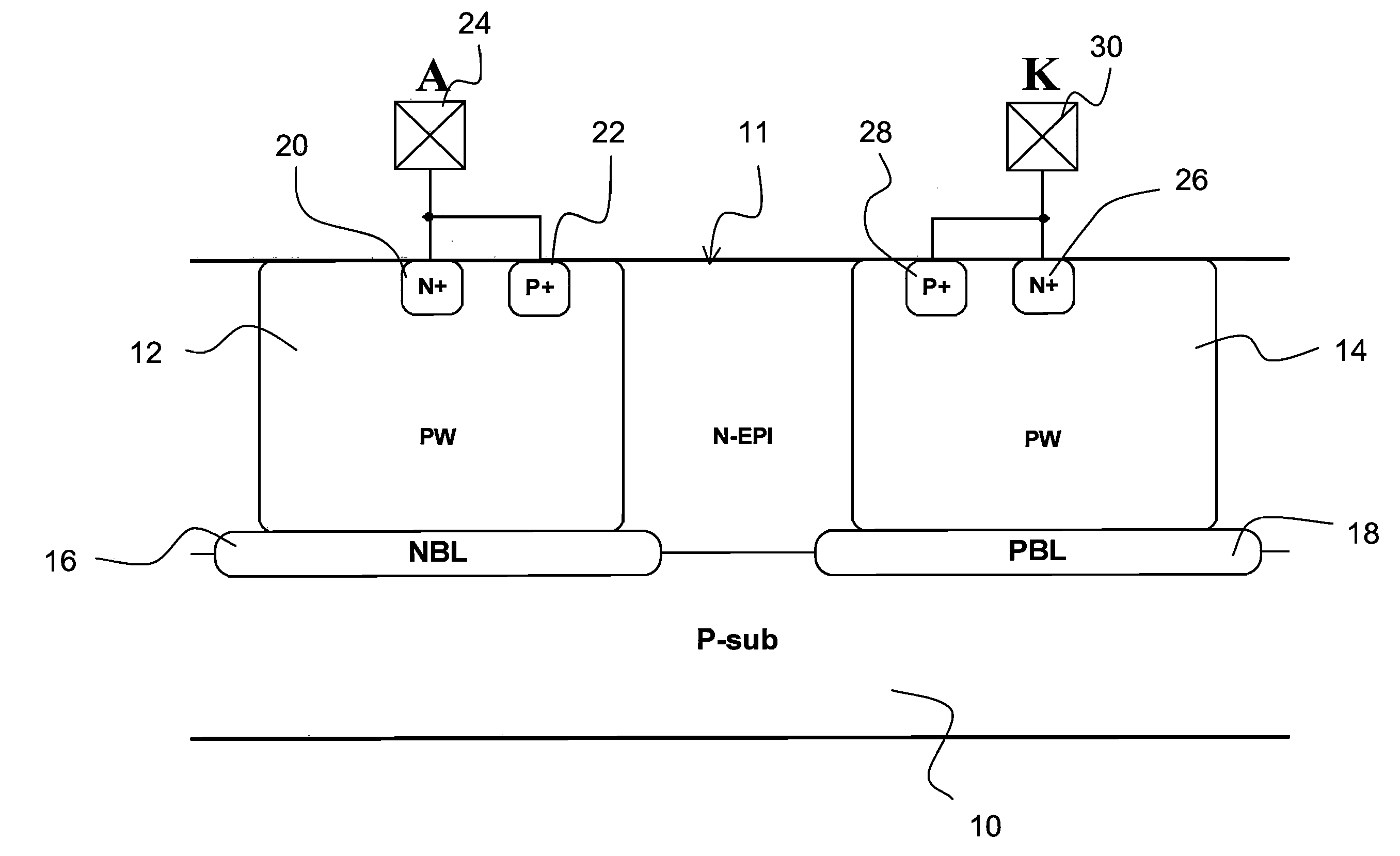
[0026]Refer to FIG. 1 a diagram schematically showing an embodiment of an asymmetric silicon-controlled rectifier according to the present invention. In this embodiment, the asymmetric silicon-controlled rectifier of the present invention comprises: a P-type substrate 10; an N-type undoped epitaxial layer 11 formed on the substrate 10; a P-type first well 12 and a P-type second well 14 formed inside the undoped epitaxial layer 11 via a doping method, wherein both sides of the first and second wells 12 and 14 have portions of the undoped epitaxial layer 11 for separation; an N-type buried layer 16 formed on the bottom of the first well 12 and a P-type buried layer 18 formed on the bottom of the second well 14; a first semiconductor area 20 and a second semiconductor area 22 respectively having a conduction type opposite to each other, wherein both of them are formed inside the first well 12 and connected to an anode 24; a third semiconductor area 26 and a fourth semiconductor area 28...


PUM


Abstract

The present invention discloses an asymmetric bidirectional silicon-controlled rectifier, which comprises: a second conduction type substrate; a first conduction type undoped epitaxial layer formed on the substrate; a first well and a second well both formed inside the undoped epitaxial layer and separated by a portion of the undoped epitaxial layer; a first buried layer formed in a junction between the first well and the substrate; a second buried layer formed in a junction between the second well and the substrate; a first and a second semiconductor area with opposite conduction type both formed inside the first well; a third and a fourth semiconductor area with opposite conduction type both formed inside the second well, wherein the first and second semiconductor areas are connected to the anode of the silicon-controlled rectifier, and the third and fourth semiconductor areas are connected to the cathode of the silicon-controlled rectifier.

Description

BACKGROUND OF THE INVENTION[0001]1. Field of the Invention[0002]The present invention relates to a silicon-controller rectifier, particularly to an asymmetric bidirectional silicon-controlled rectifier, which has a small area, adjustable trigger voltage and high electrostatic-discharge protection capability. The proposed silicon-controller rectifier can apply to an ESD protection element for I / O ports with signal of positive and negative voltage.[0003]2. Description of the Related Art[0004]With the increasing request of transistors count, CMOS(Complementary Metal Oxide Semiconductor) have been developed to a submicron or even deep-submicron scale. The thin gate oxide layer of the submicron or deep-submicron technology is easy to damage under higher voltage level. In common conditions, the electrostatic discharge (ESD) voltage may cause several thousands voltage, which will easily damage integrated circuits (IC) product.[0005]The silicon-controlled rectifier with a low turn-on resist...

Claims


Application Information

Patent Timeline
Patent Type & Authority Applications(United States)
IPC IPC(8): H01L29/747
CPCH01L27/0262H01L29/87H01L29/747
Inventor TSENG, TANG-KUEICHUANG, CHE-HAOJIANG, RYAN HSIN-CHINKER, MING-DOU
Owner AMAZING MICROELECTRONICS
Why Eureka
Try Eureka