Field effect transistor having an asymmetric gate electrode

a field effect transistor and gate electrode technology, applied in semiconductor devices, digital storage, instruments, etc., can solve the problem of limiting the performance of conventional silicon oxide based gate electrodes

Inactive Publication Date: 2009-02-05
GLOBALFOUNDRIES INC
View PDF43 Cites 22 Cited by
  • Summary
  • Abstract
  • Description
  • Claims
  • Application Information

AI Technical Summary

Benefits of technology

[0010]The gate electrode of a metal oxide semiconductor field effect transistor (MOSFET) comprises a source side gate electrode and a drain side gate electrode that abut each other near the middle of the channel. In one embodiment, the source side gate electrode comprises a silicon oxide based gate dielectric and the drain side gate electrode comprises a high-k gate dielectric. The source side gate electrode provides high carrier mobility, while the drain side gate electrode provides good short channel effect and reduced gate leakage. In another embodiment, the source gate electrode and drain gate electrode comprises different high-k gate dielectric stacks and different gate conductor materials, wherein the source side gate electrode has a first work function about a quarter band gap away from a band gap edge and the drain side gate electrode has a second work function near the band gap edge.

Problems solved by technology

High gate leakage current of nitrided silicon dioxide and depletion effect of polysilicon gate electrodes limit the performance of conventional silicon oxide based gate electrodes in metal oxide semiconductor field effect transistors (MOSFETs).

Method used


Image

  • Field effect transistor having an asymmetric gate electrode
  • Field effect transistor having an asymmetric gate electrode
  • Field effect transistor having an asymmetric gate electrode

Examples


Embodiment Construction

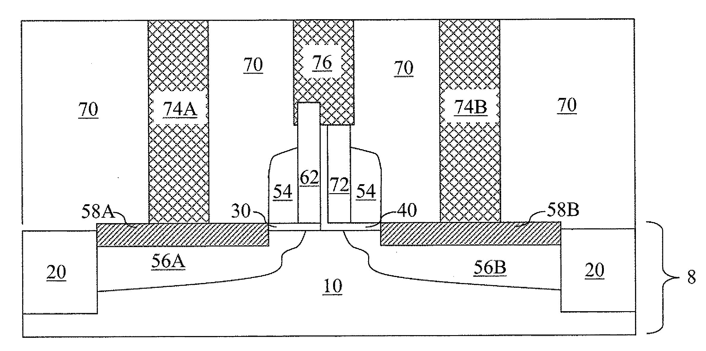
[0060]As stated above, the present invention relates to a metal oxide semiconductor field effect transistor (MOSFET) having an asymmetric gate electrode and methods of manufacturing the same, which are now described in detail with accompanying figures. It is noted that like and corresponding elements are referred to by like reference numerals.

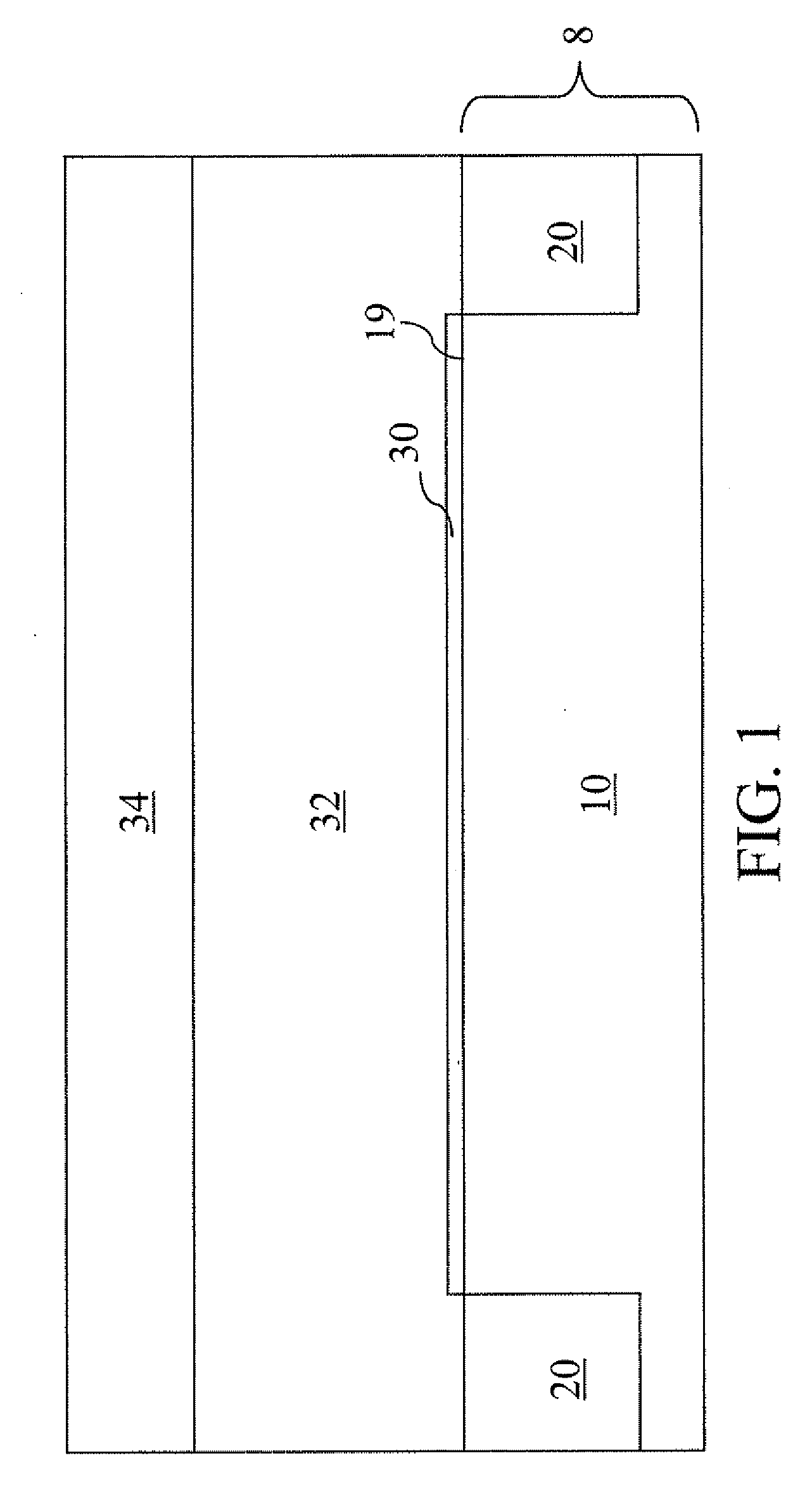
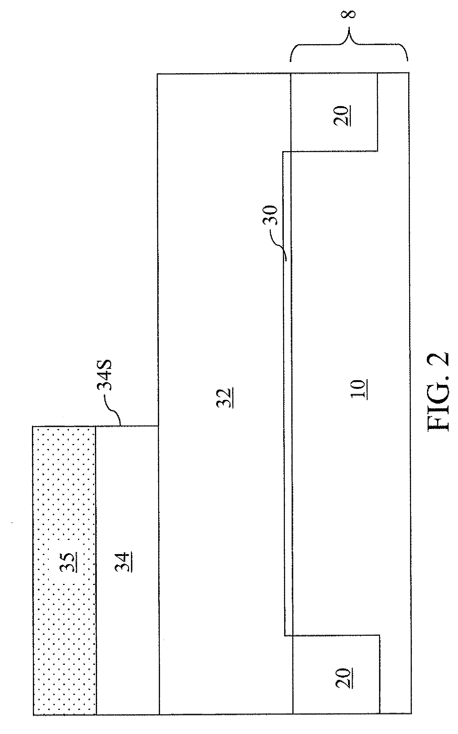
[0061]Referring to FIG. 1, a first exemplary semiconductor structure according to a first embodiment of the present invention comprises a semiconductor substrate 8 containing shallow trench isolation 20 and a substrate layer 10. The shallow trench isolation 20 comprises a dielectric material such as silicon oxide. The shallow trench isolation 20 surrounds a region of the substrate layer 10 so that a device formed in the region may be electrically isolated from other devices located on the same semiconductor substrate 8.

[0062]The substrate layer 10 comprises a semiconductor material. The semiconductor material may be selected from, but is not li...


PUM


Abstract

The gate electrode of a metal oxide semiconductor field effect transistor (MOSFET) comprises a source side gate electrode and a drain side gate electrode that abut each other near the middle of the channel. In one embodiment, the source side gate electrode comprises a silicon oxide based gate dielectric and the drain side gate electrode comprises a high-k gate dielectric. The source side gate electrode provides high carrier mobility, while the drain side gate electrode provides good short channel effect and reduced gate leakage. In another embodiment, the source gate electrode and drain gate electrode comprises different high-k gate dielectric stacks and different gate conductor materials, wherein the source side gate electrode has a first work function a quarter band gap away from a band gap edge and the drain side gate electrode has a second work function near the band gap edge.

Description

FIELD OF THE INVENTION[0001]The present invention relates to semiconductor devices, and particularly, to a metal oxide semiconductor field effect transistor (MOSFET) having an asymmetric gate electrode and methods of manufacturing the same.BACKGROUND OF THE INVENTION[0002]High gate leakage current of nitrided silicon dioxide and depletion effect of polysilicon gate electrodes limit the performance of conventional silicon oxide based gate electrodes in metal oxide semiconductor field effect transistors (MOSFETs). High performance devices for an equivalent oxide thickness (EOT) less than 1 nm require high dielectric constant (high-k) gate dielectrics and metal gate electrodes to limit the gate leakage current and provide high on-currents. The high-k gate dielectrics have demonstrated improvement in short channel effects in transistors having a gate length less than 65 nm compared with conventional silicon oxide based gate dielectrics.[0003]A high-k dielectric material needs to provide...

Claims


Application Information

Patent Timeline
Patent Type & Authority Applications(United States)
IPC IPC(8): H01L29/78H01L21/336
CPCH01L21/28105H01L21/28114H01L21/28132H01L29/42376H01L29/4983H01L21/28008H01L29/517H01L29/66484H01L29/665H01L29/66613H01L29/7831H01L29/512
Inventor ZHU, HUILONGLIANG, QINGQING
Owner GLOBALFOUNDRIES INC
Why Eureka
Try Eureka