Thin Film Solar Cell III

Inactive Publication Date: 2009-02-12
TRANSLUCENT
View PDF7 Cites 60 Cited by
  • Summary
  • Abstract
  • Description
  • Claims
  • Application Information

AI Technical Summary

Benefits of technology

[0025]Therefore, there is a need for a low cost, high throughput, large area handling manufacturing technique for producing thin films of high quality sc-Si.
[0026]Furthermore, there is a need for a cost effective, high throughput, and large area handling manufacturing technique for producing thin films of high quality sc-Si disposed upon low cost substrates.
[0027]There is also a need for a cost effective, high throughput, and large area handling manufacturing technique for creating la

Problems solved by technology

Generally, prior art approaches at generating thin films of sc-Si have been limited via mechanical sawing of bulk Si material and/or deposit

Method used


Image

  • Thin Film Solar Cell III
  • Thin Film Solar Cell III
  • Thin Film Solar Cell III

Examples


example 1

Thin Film Solar Vertical Process

[0141]In one embodiment a disclosed process is used to fabricate a vertical type opto-electronic solar spectrum energy conversion device using thin film single crystal Si layer transfer method. FIGS. 8A and B shows the individual parallel process paths for fabrication of thin film solar cell article. A single crystal CZ Si substrate 801 and alternative substrate 807 are cleaned and prepared for processing. An protective layer 802, optionally SiO2, is deposited or thermally grown on the CZ Si substrate 801. The CZ substrate is then implanted according to the method described in the present invention to form a buried defect layer 804. The layer 802 is removed via wet or dry etch or other means known to one knowledgeable in the art. The cleaned alternative substrate is then deposited with a uniform conductive layer 808, for example metal such as aluminum and / or rare-earth metal.

[0142]FIG. 9 shows how the alternative substrate with conductive layer 809 an...

example 2

Thin Film Solar Planar Process

[0147]In one embodiment a disclosed process is used to fabricate a planar type opto-electronic solar spectrum energy conversion device using thin film single crystal Si layer transfer method. A key feature of this process is the extensive use of selective patterning of electrical contacts to form planar buried contact arrangement to a interface of the CZ Si thin film active layer.

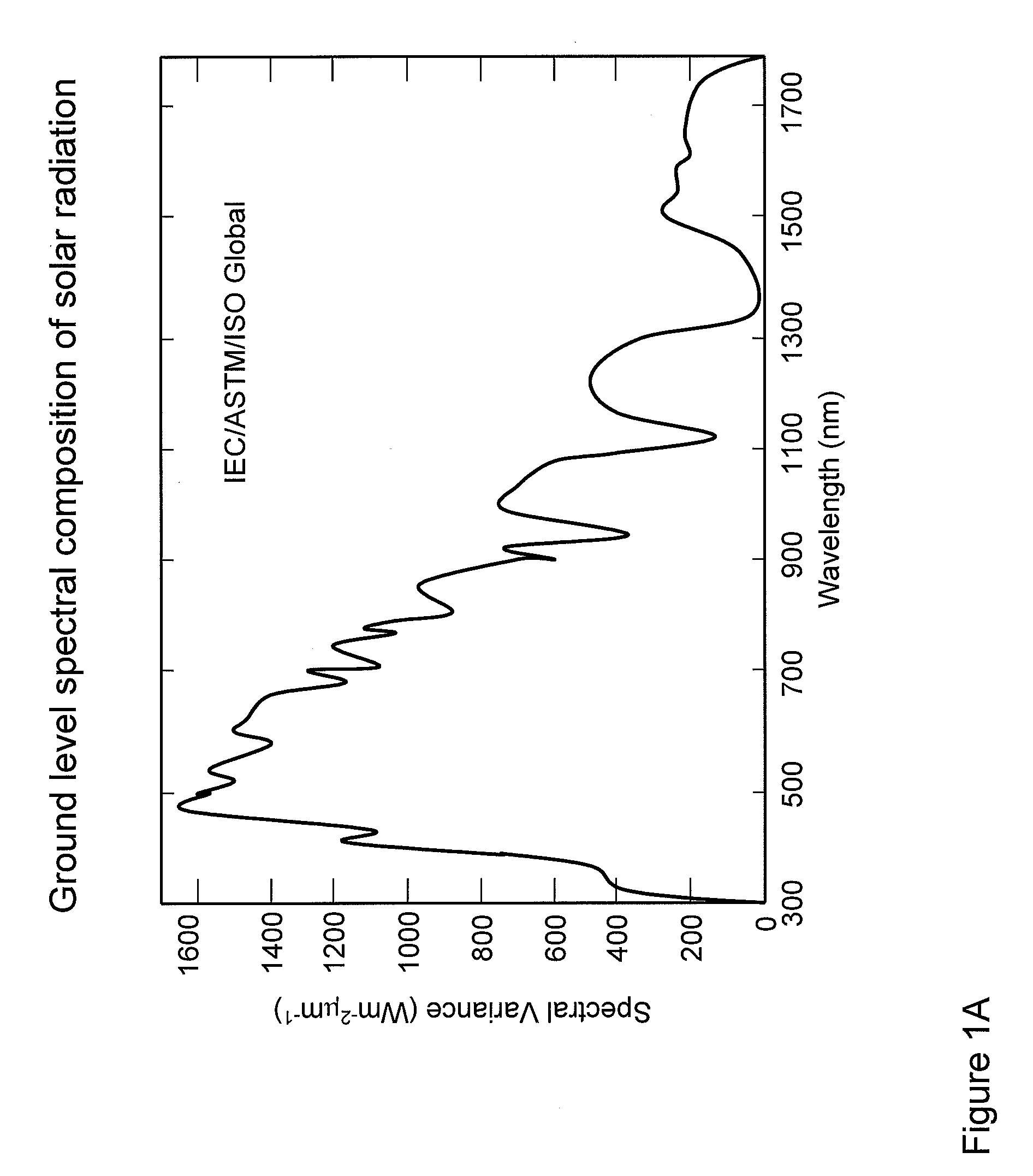
[0148]This planar contact arrangement is suitable for optimized metal-semiconductor-metal (MSM) inter-digitated finger configurations. The shorter wavelengths (i.e., high energy) of the solar spectrum contains the majority of the solar spectrum fluence. Typically, high energy photons, particularly UV photons, are considered detrimental to the performance of single junction solar cells, particularly using Si (refer FIG. 4). The present invention solves this long standing problem by utilizing the wavelength selective nature of absorption of photons in the Si crystal. Silicon SJ s...

example 3

Thin Film Solar Planar Process

[0159]In one embodiment a disclosed process is used to fabricate a planar type opto-electronic solar spectrum energy conversion device using thin film single crystal Si layer transfer method. A key feature of this process is the extensive use of ion implantation to affect the conductivity type of selective regions within the CZ Si thin film active layer. The electronic structures possible are discussed later and disclosed in FIGS. 44 to 51, inclusive.

[0160]FIGS. 18 to 26 disclose the individual process paths for fabrication of thin film solar cell article and wafer scale solar energy conversion modules.

[0161]FIG. 18 shows initial processing steps of the alternative substrate containing patterned planar electrodes. Cleaned alternative substrate 1806 is deposited with spatially patterned conductive layers 1807 and 1808, for example metals such as aluminum (Al) and / or rare-earth (RE) metal. If separate metals are used for 1807 and 1808, they can be deposit...


PUM


Abstract

The present invention teaches a device for converting solar radiation to electrical energy comprising a thin film, single crystal device chosen from a variety of semiconductor materials, optionally, employing an alternative substrate, and various combinations of p-n, p-i-n and avalanche p-i-n diodes to enable high conversion efficiency photo-voltaic devices.

Description

CROSS REFERENCE TO RELATED APPLICATIONS[0001]Applications and patent Ser. Nos. 09 / 924,392, 10 / 666,897, 10 / 746,957, 10 / 799,549, 10 / 825,912, 10 / 825,974, 11 / 022,078, 11 / 025,363, 11 / 025,680, 11 / 025,681, 11 / 025,692, 11 / 025,693, 11 / 084,486, 11 / 121,737, 11 / 187,213, U.S. 20050166834, U.S. 20050161773, U.S. 20050163692, 11 / 053,775, 11 / 053,785, 11 / 054,573, 11 / 054,579, 11 / 054,627, 11 / 068,222, 11 / 188,081, 11 / 253,525, 11 / 254,031, 11 / 257,517, 11 / 257,597, 11 / 393,629, 11 / 398,910, 11 / 472,087, 11 / 788,153, 60 / 533,378, 60 / 811,311, 60 / 820,438, 60 / 847,767, 60 / 876,182, 60 / 905,415, 60 / 944,369, 60 / 949,753, U.S. Pat. No. 7,018,484, U.S. Pat. No. 6,734,453, U.S. Pat. No. 7,023,011, U.S. Pat. No. 6,858,864, U.S. Pat. No. 7,037,806, U.S. Pat. No. 7,135,699, and U.S. Pat. No. 7,199,015, all held by the same assignee, contain information relevant to the instant invention and are included herein in their entirety by reference. “Thin Film Silicon Energy Conversion Devices”, which is attached, is included herein by ...

Claims


Application Information

Patent Timeline
IPC IPC(8): H01L31/00
CPCH01L21/76254H01L31/02021H01L31/022425H01L31/028Y02E10/547H01L31/0304H01L31/03529Y02E10/544H01L31/0296Y02P70/50
Inventor ATANACKOVIC, PETAR B.
Owner TRANSLUCENT
Why Eureka
Try Eureka