Semiconductor device and method of manufacturing the same

a semiconductor and semiconductor technology, applied in the direction of semiconductor devices, electrical equipment, transistors, etc., can solve the problems of difficult junction leakage reduction, many defects in the silicon nitride film that covers the side surfaces of the refractory metal film, etc., and achieve the effect of effectively preventing the scattering of refractory metal

Active Publication Date: 2009-02-12
LONGITUDE LICENSING LTD
View PDF7 Cites 0 Cited by
  • Summary
  • Abstract
  • Description
  • Claims
  • Application Information

AI Technical Summary

Benefits of technology

[0007]It is therefore an object of the present invention to provide a semiconductor device that can reduce a junction leakage of a MOSFET having a gate electrode of a poly-metal structure, particularly, a memory cell transistor of a DRAM.
[0010]According to the present invention, the sidewall that covers the side surfaces of the poly-metal gate electrode has a multilayer structure. Therefore, serious defects do not occur in the sidewall. Consequently, it is possible to effectively prevent a scattering of the refractory metal contained in the poly-metal gate electrode. Accordingly, junction leakage attributable to the refractory metal can be reduced substantially.
[0011]In order to reinforce the sidewall, there is also considered a method of increasing a film thickness of the sidewall in a single-layer structure, instead of in a multilayer structure as in the present invention. However, according to this method, the amount of etch back increases corresponding to the increased film thickness, and the damage on the sidewall increases. On the other hand, based on the structure of the sidewall according to the present invention, at the time of etching back the external dielectric film (the second dielectric film, for example), little damage is caused on the internal dielectric film (the first dielectric film, for example). At the time of etching the internal dielectric film (the first dielectric film), a part covered with the external dielectric film (the second dielectric film) is protected. Consequently, a sidewall (the first dielectric film) with a very small amount of defects can be finally obtained.
[0013]According to the present invention, the poly-silicon film is patterned and the light oxidation is carried out after the sidewalls having a multilayer structure are formed on the side surfaces of the refractory metal film. Therefore, a scattering of the refractory metal can be effectively prevented at the time of light oxidizing the poly-silicon film.
[0014]The fourth step can include: a step of depositing a silicon nitride film; a step of depositing a silicon oxide film on the silicon nitride film; a step of etching back the silicon oxide film; and a step of etching the silicon nitride film using the silicon oxide film as a mask. Based on this arrangement, the silicon nitride film is hardly damaged at the time of etching back the silicon oxide film. Further, at the time of etching the silicon nitride film, the part covered with the silicon oxide film is protected. Accordingly, a sidewall (silicon nitride film) with a very small amount of defects can be formed.

Problems solved by technology

However, according to researches carried out by the inventors of the invention, it is made clear that it is difficult to reduce a junction leakage to a predetermined level or lower even when a light oxidation is carried out after covering the side surfaces of a refractory metal film with a silicon nitride film.
It is found through the research that the silicon nitride film that covers the side surfaces of the refractory metal film has many defects.
These defects are considered to be attributable to damages caused, by etching, to a part where the silicon nitride film remains to cover the side surfaces of the refractory metal film, at the time of etching back the silicon nitride film.

Method used


Image

  • Semiconductor device and method of manufacturing the same
  • Semiconductor device and method of manufacturing the same
  • Semiconductor device and method of manufacturing the same

Examples


Embodiment Construction

[0037]Preferred embodiments of the present invention will now be described in detail with reference to the accompanying drawings.

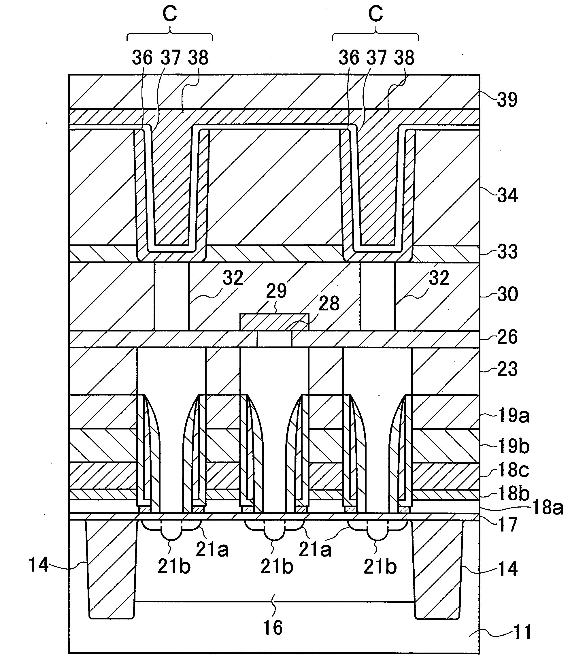
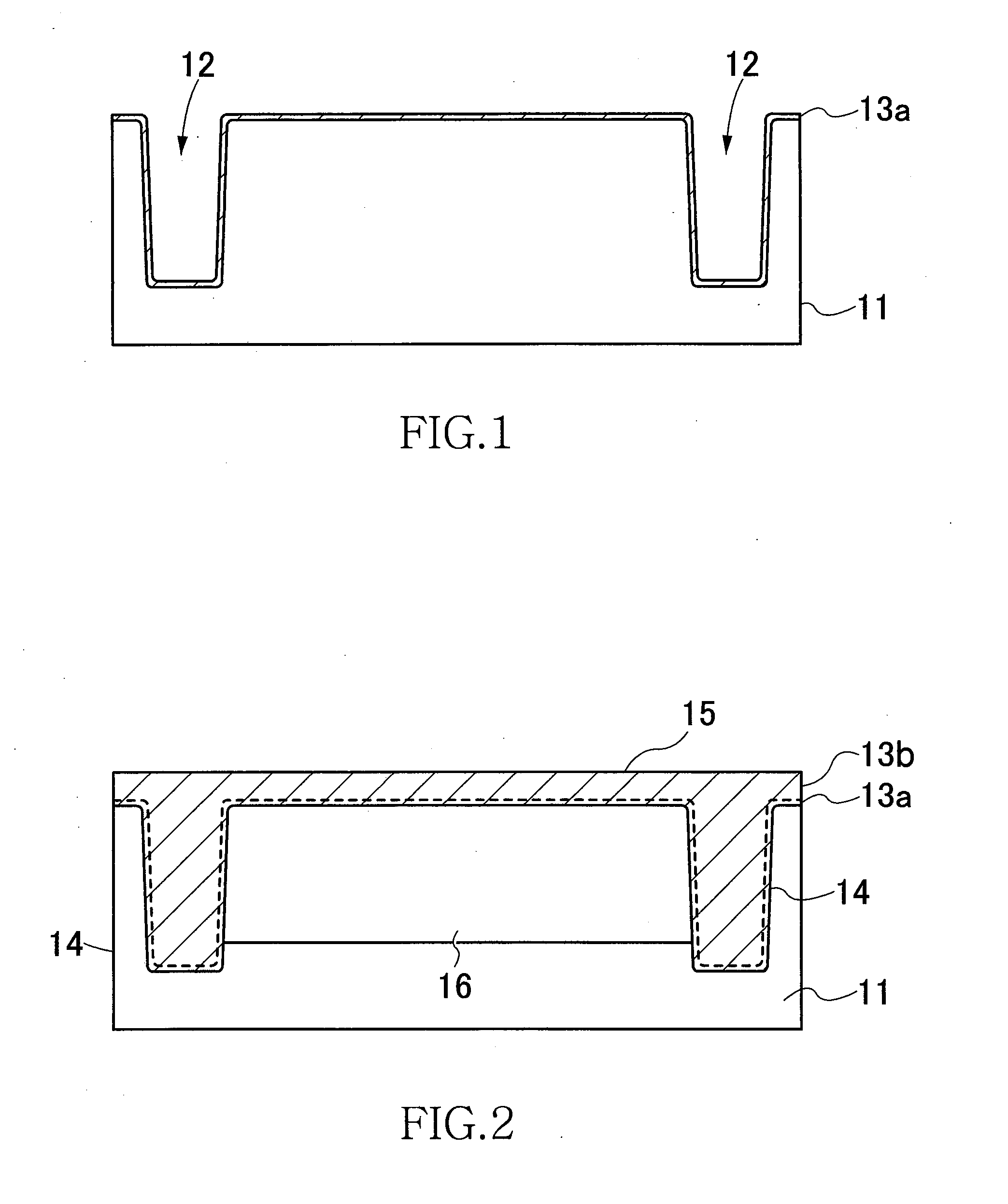
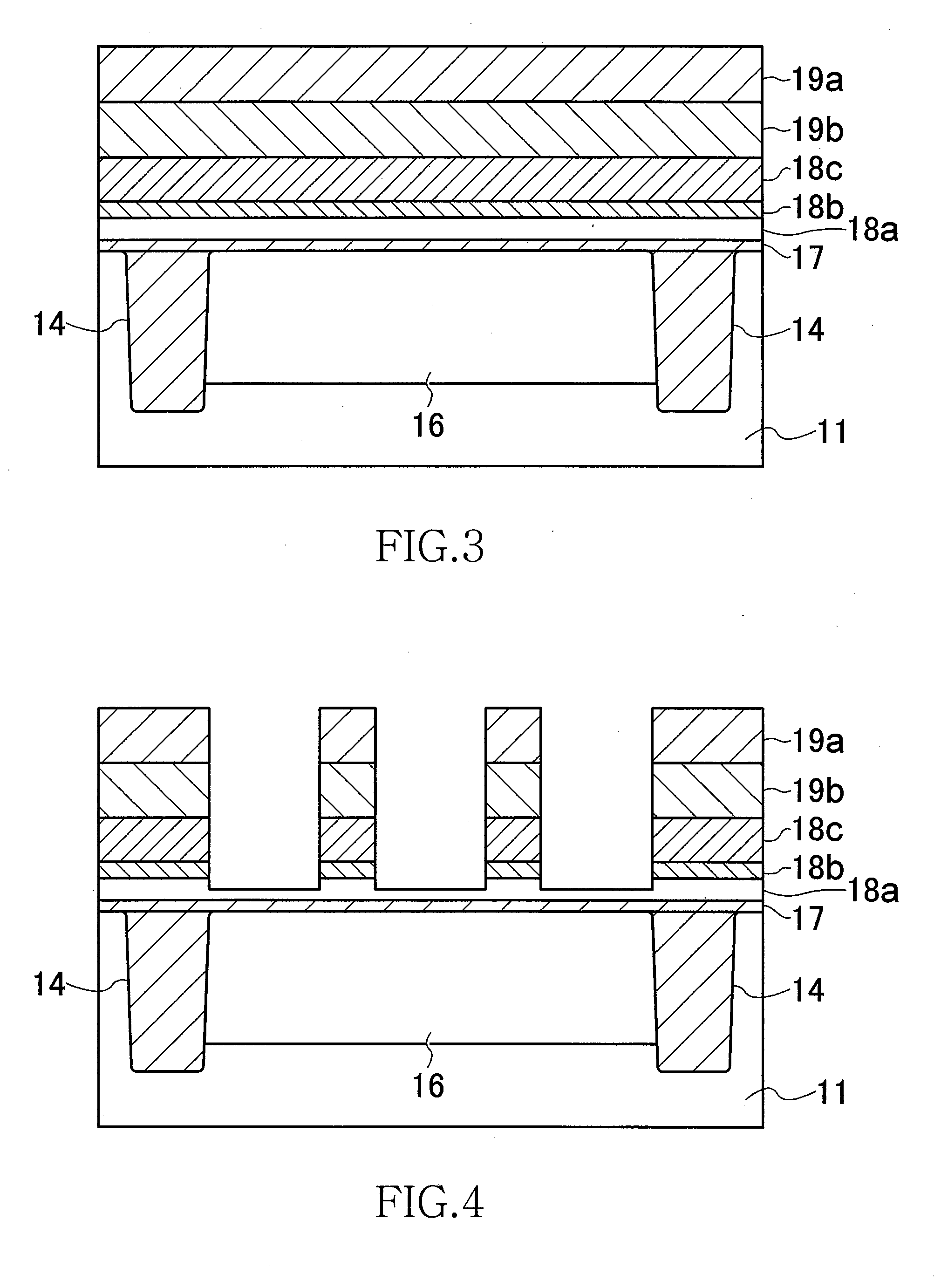
[0038]FIG. 1 to FIG. 21 is schematic cross sections of processes of a method of manufacturing a semiconductor device according to the exemplary embodiment of the present invention. In the present embodiment, the manufacturing method according to the present invention is applied to a DRAM.

[0039]First, as shown in FIG. 1, a semiconductor substrate 11 made of p-type mono-crystalline silicon having a specific resistance of about 1 to 10 Ω / cm is etched, thereby forming an element isolation trench 12 having a depth of about 350 nm. The semiconductor substrate 11 is thermally oxidized at about 1,000° C., thereby forming a silicon oxide film 13a as thin as about 10 nm on an inner wall of the element isolation trench 12. This silicon oxide film 13a is formed to repair a damage generated on the inner wall of the element isolation trench 12 due to the etching, and to...


PUM

PropertyMeasurementUnit
depthaaaaaaaaaa
thicknessaaaaaaaaaa
thicknessaaaaaaaaaa

Abstract

A gate dielectric film, a poly-silicon film, a film of a refractory metal such as tungsten, and a gate cap dielectric film are sequentially laminated on a semiconductor substrate. The gate cap dielectric film and the refractory metal film are selectively removed by etching. Thereafter, a double protection film including a silicon nitride film and a silicon oxide film is formed on side surfaces of the gate cap dielectric film, the refractory metal film, and the poly-silicon film. The poly-silicon film is etched using the double protection film as a mask. Thereafter, the semiconductor substrate is light oxidized to form a silicon oxide film on side surfaces of the poly-silicon film. Accordingly, a junction leakage of a MOSFET having a gate electrode of a poly-metal structure, particularly, a memory cell transistor of a DRAM, can be further reduced.

Description

FIELD OF THE INVENTION[0001]The present invention relates to a semiconductor device and a method of manufacturing the same. The invention particularly relates to a metal-oxide semiconductor field-effect transistor (MOSFET) having a gate electrode of a poly-metal structure consisting of high-melting point metal and polycrystalline silicon (poly-silicon), and a method of manufacturing the MOSFET.BACKGROUND OF THE INVENTION[0002]Recently, in a MOSFET that is used for a memory cell such as a dynamic random access memory (DRAM), a so-called poly-metal structure gate electrode (poly-metal gate) having a refractory metal film such as tungsten stacked on a poly-silicon film is used in order to reduce resistance of a gate electrode (see Japanese Patent Application Laid-Open Nos. 2000-156497 and 2002-141500).[0003]On the other hand, at the time of patterning the gate electrode, a gate dielectric film positioned at a lower part of the gate electrode is also slightly etched. Therefore, a breakd...

Claims


Application Information

Patent Timeline
Patent Type & Authority Applications(United States)
IPC IPC(8): H01L21/28
CPCH01L21/28044H01L21/28114H01L29/7833H01L29/6659H01L29/42376
Inventor OYU, KIYONORIOKONOGI, KENSUKE
Owner LONGITUDE LICENSING LTD
Why Eureka
Try Eureka