Etchant for silicon wafer surface shape control and method for manufacturing silicon wafers using the same

a technology of surface shape and control method, which is applied in the direction of basic electric elements, electrical apparatus, chemistry apparatus and processes, etc., can solve the problems of reducing the mechanical strength of the wafer, adversely affecting the electrical characteristics, and damaged layers, so as to maintain the flat reduce the roughness of the wafer front side, and maintain the flatness

Inactive Publication Date: 2009-02-12
SUMCO CORP
View PDF3 Cites 14 Cited by
  • Summary
  • Abstract
  • Description
  • Claims
  • Application Information

AI Technical Summary

Benefits of technology

[0023]The etchant for controlling a silicon wafer surface shape of the present invention is an etchant in which the fluorochemical surfactant is uniformly mixed in the alkaline aqueous solution, and this etchant can control the front side roughness and the texture size of the wafer before polishing, so that etching the silicon wafer with the work-affected layer, to which the flattening process has been subjected, using this etchant, makes it possible to achieve both of the maintenance of the wafer flatness and the reduction in wafer front side roughness upon completing the flattening process while reducing the polishing removal allowances on the front and back sides of the wafer in a both-side simultaneous polishing process or a single-side polishing process, respectively.
[0024]Moreover, in the method for manufacturing the silicon wafers according to the present invention, since the front side roughness and the texture size of the wafer before polishing can be controlled by the etching process using the adjusted etchant in which the fluorochemical surfactant is added to the alkaline aqueous solution, it is possible to achieve both of the maintenance of the wafer flatness and the reduction in wafer front side roughness upon completing the flattening process while reducing polishing removal allowances on the front and back sides of the wafer in a both-side simultaneous polishing process or a single-side polishing process, respectively.

Problems solved by technology

The silicon wafers, which have passed through mechanical manufacturing processes, such as block cutting, outer diameter grinding, slicing, and lapping, have damaged layers, namely, work-affected layers, on the surface thereof.
Since the work-affected layer causes crystal defects, such as a slip dislocation or the like during device manufacturing processes, reduces mechanical strength of the wafer and adversely influences on electrical characteristics thereof, it must be completely removed.
In this acid etching, however, although the work-affected layer can be etched while improving the front side roughness of the silicon wafer, an outer circumferential portion of the wafer becomes dull as the acid etching progresses on, and the flatness which is a macroscopic shape precision obtained by the lapping is impaired, causing problems that unevenness called waves or peels in a range of mm order on an etched surface.
Further, there have been disadvantages that a cost of a chemical liquid is high, and in addition to that, it is difficult to control and maintain the composition of the etchant.
In the alkali etching, however, although the work-affected layer can be etched while maintaining the flatness of the silicon wafer, pits (Hereinafter, these are called facets.) with a partial depth of several micrometers and a size of about several to several tens of micrometers are generated, causing problems that the wafer front side roughness is deteriorated.
In the conventional methods including the method shown in the above-mentioned Patent Document 1, however, although the etched wafer is subjected to a both-side simultaneous polishing process or a single-side polishing process to thereby make the front side thereof into a mirror plane the wafer flatness upon completing a flattening process cannot be maintained and the desired wafer front side roughness is not obtained, either, on front and back sides of a silicon wafer which has been subjected to an etching process, and thus in order to improve the wafer flatness and the wafer front side roughness, it is necessary to take large polishing removal allowances in the both-side simultaneous polishing process or the single-side polishing process, thereby high workload has been imposed on the both-side simultaneous polishing process or the single-side polishing process.

Method used


Image

  • Etchant for silicon wafer surface shape control and method for manufacturing silicon wafers using the same
  • Etchant for silicon wafer surface shape control and method for manufacturing silicon wafers using the same
  • Etchant for silicon wafer surface shape control and method for manufacturing silicon wafers using the same

Examples


example

[0046]Next, examples of the present invention will be described in detail with comparative examples.

examples 1 through 5

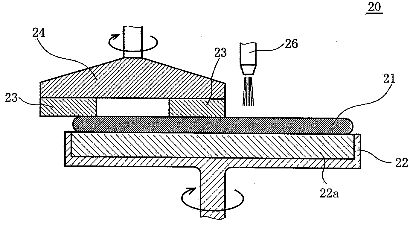
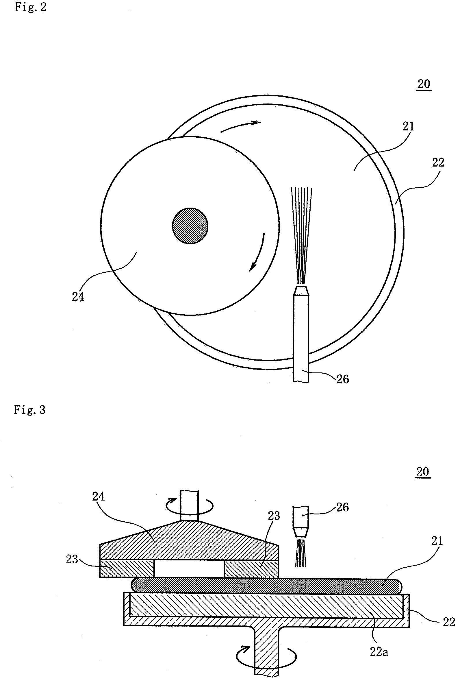
[0047]First, a plurality of silicon wafers of 200 mm diameter are prepared, and the front and back sides of the silicon wafers are subjected to lapping using the lapping apparatus shown in FIG. 4 as the flattening process. An abrasive material including Al2O3 whose count is #1500 is used for the abrasive material in the lapping process, and the silicon wafers are flattened while a flow rate of the abrasive material to be supplied is controlled to be 2.0 L / min, a load of the upper surface table, 70 g / cm2; a rotational frequency of the upper surface table, 10 rpm; and a rotational frequency of the lower surface table, 40 rpm, respectively. Next, as the etching process, the silicon wafers after being flattened are subjected to etching using an etching system shown in FIG. 5. Five types of etchants, in which C8F17SO3K (made by MITSUBISHI MATERIALS CORP., brand name; EFTOP EF-102) as a surfactant is mixed into 50 weight percent sodium hydroxide and prepared so as to be 15 g / L (1:100), 1....

examples 6 through 10

[0048]The flattening process and the etching process are performed in a manner similar to those of the examples 1 through 5 other than replacing the alkaline aqueous solution used for the etchant in the etching process with 40 weight percent aqueous sodium hydroxide solution.


PUM

PropertyMeasurementUnit
weight percentaaaaaaaaaa
diameteraaaaaaaaaa
flow rateaaaaaaaaaa

Abstract

It is possible to reduce workloads of a both-side simultaneous polishing process or a single-side polishing process, and to achieve both of the maintenance of the wafer flatness and the reduction in wafer front side roughness upon completing a flattening process. A method for manufacturing silicon wafers according to the present invention includes a flattening process 13 of grinding or lapping front and back sides of a thin disc-shaped silicon wafer obtained by slicing a silicon single crystal ingot, an etching process of immersing the silicon wafer in an etchant for controlling a silicon wafer surface shape in which a fluorochemical surfactant is uniformly mixed in an alkaline aqueous solution to etch the front and back sides of the silicon wafer, and a both-side simultaneous polishing process 16 of simultaneously polishing the front and back sides of the etched silicon wafer or a single-side polishing process of polishing the front and back sides of the etched wafer for every side, in this order.

Description

BACKGROUND OF THE INVENTION[0001]1. Field of the Invention[0002]The present invention relates to an etchant for controlling a silicon wafer surface shape and a method for manufacturing silicon wafers using the etchant, which are capable of reducing workloads of a both-side simultaneous polishing process, and achieving both of the high flatness and the reduction in front side roughness.[0003]2. Description of the Related Art[0004]Generally, a manufacturing process of semiconductor silicon wafers is composed of processes of chamfering, mechanically polishing (lapping), etching, mirror-polishing (polishing) and cleaning wafers obtained by cutting and slicing a pulled silicon single crystal ingot, and produces wafers having highly precise flatness. The silicon wafers, which have passed through mechanical manufacturing processes, such as block cutting, outer diameter grinding, slicing, and lapping, have damaged layers, namely, work-affected layers, on the surface thereof. Since the work-...

Claims


Application Information

Patent Timeline
Patent Type & Authority Applications(United States)
IPC IPC(8): H01L21/302C09K13/08
CPCC09K13/02H01L21/30608H01L21/02019C09K13/08
Inventor KOYATA, SAKAEKATOH, TAKEOHASHII, TOMOHIROMURAYAMA, KATSUHIKOTAKAISHI, KAZUSHIGE
Owner SUMCO CORP
Why Eureka
Try Eureka