Electrically and Thermally Non-Metallic Conductive Nanostructure-Based Adapters

a nanostructure and adapter technology, applied in the direction of non-conductive materials with dispersed conductive materials, connection contact member materials, soldered/welded conductive connections, etc., can solve the problems of difficult to provide a good contact at the junction of an integrated circuit housing, difficult to provide a good contact area, and severe degrading the performance of capacitors. , to achieve the effect of low resistance coupling

Active Publication Date: 2009-02-12
NANCOMP TECHNOLOGIES INC
View PDF105 Cites 33 Cited by
  • Summary
  • Abstract
  • Description
  • Claims
  • Application Information

AI Technical Summary

Benefits of technology

[0012]The present invention provides, in accordance with one embodiment, a conductive adapter. The adapter includes, in an embodiment, a conducting member made from a conductive nanostructure-based material and having opposing ends. Such a material may be wires, yarns, tapes, ribbons or sheets made from carbon nanotubes. In an embodiment, the conducting member can be made from one of carbon, copper, silver, boron, boron-nitride, MoS2 or similar compounds, or a combination thereof. The adapter can also include a connector portion positioned on one end of the conducting member for maximizing a number of conductive nanostructures within the conducting member in contact with connector portion, so as to enable efficient conduction between a nanoscale environment and a traditional electrical and/or thermal circuit system. In one embodiment, the connector portion may be made from o...

Problems solved by technology

This type of binding system can generate a substantially high internal resistance that can severely degrade the performance of the capacitor.
In the case of thermal junctions, the provision of good contact area can often be difficult.
For example, it can be difficult to provide a good contact at the junction between an integrated circuit housing and a heat sink, where a thermal resistance of more than 20 degrees may be needed to drive, for instance, 150 watts per square cm though the junction.
This limitation of the total surface area that may be in actual contact between a connector and its corresponding contacting element can generally introduce a severe electrical or thermal contact resistance.
However, the lead-tin alloys in common use for soldering, or even lead free solders (e.g., silver-...

Method used


Image

  • Electrically and Thermally Non-Metallic Conductive Nanostructure-Based Adapters
  • Electrically and Thermally Non-Metallic Conductive Nanostructure-Based Adapters
  • Electrically and Thermally Non-Metallic Conductive Nanostructure-Based Adapters

Examples


example i

[0057]Wires for use as current conducting members can be made from yarns that have been fabricated using carbon nanotubes of the present invention. In one embodiment, a plurality of carbon nanotube yarns was coated with a glassy carbon resin and bonded together to form a wire. The wire was then heated to about 125° C. for about one hour. Following this heating step, the wire was transferred to a high temperature furnace where it was heated to a temperature at least 450° C. for about another hour in an inert atmosphere.

[0058]Wires made from carbon nanotube yarns were observed to have a resistivity in the semiconducting member state of about 0.5×10⁻⁵ to about 4×10⁻⁴.

[0059]The thermal conductivity of the wires made from carbon nanotube yarns was also measured. In an example, the thermal conductivity of wires made from carbon nanotube yarns were observed to be between about 5 Watts / meter-degree K and about 70 Watts / meter-degree K. This wide variation in thermal conductivity may be a...

example ii

[0062]In the same way as the wires above, carbon nanotube tapes or ribbons can be made from strips of carbon nanotube textiles. In one embodiment, a plurality of the strips were joined together by coating a surface of each strip with furfuryl alcohol (i.e., glassy carbon precursor), then mechanically compressing the joint between adjacent strips. The amount of glassy carbon precursor added to the strips depends on the thickness of the strips. For optimal conduction, the joints should be saturated. While compressing, the joined strips (i.e., tape or ribbon) was heated to about 125° C. for about one hour. Following this heating step, the tape or ribbon was transferred to a high temperature furnace where it was heated to a temperature at least 450° C. for about another hour in an inert atmosphere.

[0063]The resulting tape or ribbon can serve as (i) high current conducting members for high frequency transport of, for instance, very high frequency signals, as well as (ii) very efficient h...

example iii

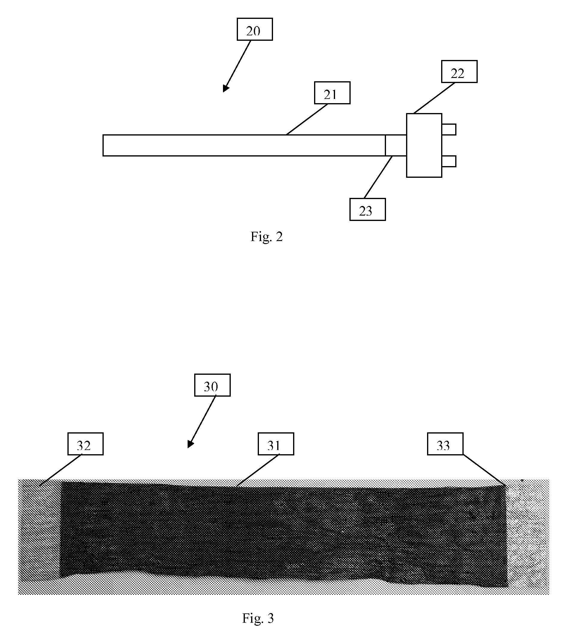
[0066]Joining of the above wires, tapes, yarns, ribbons or multiple ribbon conducting members to standard connectors (i.e., connector portions) can be also be carried out in accordance with the following method of the present invention.

[0067]In one embodiment, the insides of contact surfaces of a connector portion can be coated with, for example, malic acid (1%) catalyzed furfuryl alcohol. Then, the wire, yarn, tape or ribbon conducting member was inserted into the connector portion. The connector portion was then heated to about 125° C. for about one hour. Thereafter, the temperature was increase to about 450° C. for at least on hour in an inert gas environment.

[0068]The resulting wire, yarn, tape or ribbon conducting member having a commonly used end connector portion can be utilized to enable efficient interaction between a nanoscale environment and the traditional electrical and / or thermal circuit system.


PUM


Abstract

A conductive adapter for carrying relatively high current from a source to an external circuit without degradation is provided. The adapter includes a conducting member made from a conductive nanostructure-based material and having opposing ends. The adapter can also include a connector portion positioned on one end of the conducting member for maximizing a number of conductive nanostructures within the conducting member in contact with connector portion, so as to enable efficient conduction between a nanoscale environment and a traditional electrical and/or thermal circuit system. The adapter can further include a coupling mechanism situated between the conducting member and the connector portion, to provide a substantially uniform contact between the conductive nanostructure-based material in the conducting member and the connector portion. A method for making such a conductive adapter is also provided.

Description

RELATED U.S. APPLICATION(S)[0001]The present invention claims priority to U.S. Provisional Application Ser. Nos. 60 / 963,860, filed Aug. 7, 2007, and 61 / 044,354, filed Apr. 11, 2008, both of which are hereby incorporated herein by reference.TECHNICAL FIELD[0002]The present invention relates to electrical and thermal adapters, and more particularly, to nanostructure-based adapters designed to maximize interaction between a nanoscale conductive element and a traditional electrical and / or thermal circuit system.BACKGROUND ART[0003]The joining of electrical conductors to another element, such as a connector, in a system usually involves the use of an adhesive, and / or the use of mechanical means, such as crimping or a solder connection. All of these have some disadvantages.Adhesives[0004]Electrical or thermal contact between elements can sometimes be provided by means of an adhesive. For example, a joint between a high surface area element in an electrolytic capacitor may be formed by mea...

Claims


Application Information

Patent Timeline
IPC IPC(8): H01R4/02
CPCH01R4/58H01B1/24H01B13/0016
Inventor MANN, JENNIFERLASHMORE, DAVID S.WHITE, BRIAN
Owner NANCOMP TECHNOLOGIES INC
Why Eureka
Try Eureka