

Wafer holder for wafer prober and wafer prober equipped with same
a technology of wafer probe and probe pin, which is applied in the heating arrangement of hot plates, individual semiconductor device testing, instruments, etc., can solve the problems of long heating time, large heat generation, and contact failure between the wafer and the probe pin, so as to improve the heat insulating effect, increase the heat insulation effect, and improve the position accuracy.
- Summary
- Abstract
- Description
- Claims
- Application Information
AI Technical Summary
Benefits of technology
Problems solved by technology
Method used
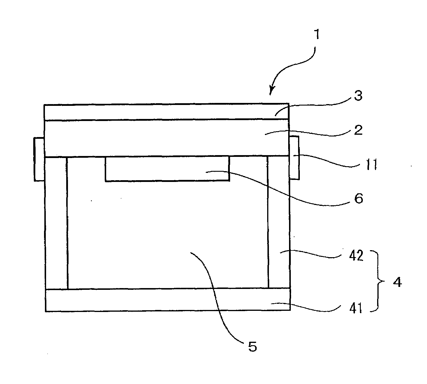
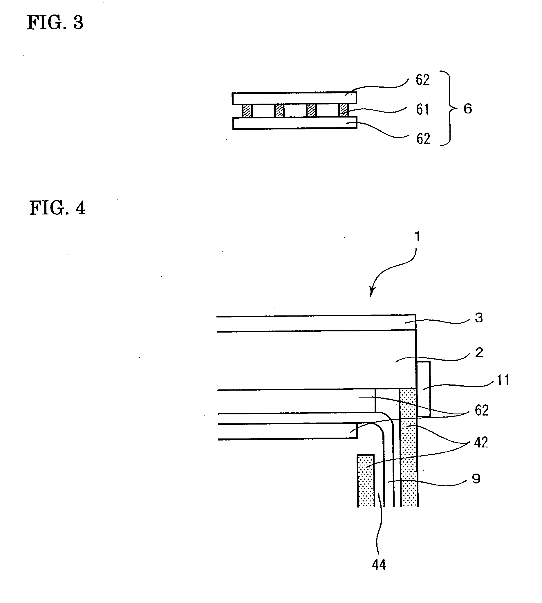
Image


Examples
working example 1
[0097]An alumina substrate was prepared with a purity of 99.5%, a diameter of 310 mm, and a thickness of 15 mm. Concentric grooves for vacuum chucking the wafer and a through hole were formed in the wafer mounting surface of the alumina substrate, and that surface was then nickel plated to form a chuck top conducting layer. Subsequently, the chuck top was completed by polishing the wafer mounting surface so that the overall warpage was 10 μm and the surface roughness Ra was 0.02 μm.
[0098]Next, a columnar mullite-alumina composite with a diameter of 310 mm, a thickness of 40 mm, and a thermal conductivity of 30 W / mK was prepared as the support member. After finishing the bottom surface of the support member and the surface of the support member that contacts the chuck top so that their flatnesses were 0.09 mm, the surface of the support member on the chuck top side was counterbored to a depth of 20 mm with an inner diameter of 295 mm, and the support member and the chuck top were ass...
working example 2
[0103]As shown in FIG. 2, excepting the fact that 32 mullite-alumina composite pillar members 23, each with a diameter of 10 mm and a thickness of 2 mm, were installed equally spaced in the circumferential direction between the chuck top and the support member, the wafer holder was prepared in the same manner as the Working Example 1, and the cooling time was measured the same as in the Working Example 1. The results are shown in Table 2.
TABLE 2Restricting MemberFillerCooling TimeNoneNoneDid not reach −55° C.even at 60 minStainless steelNone40 minStainless steelSilicone resin35 minPolyimideNone39 minPolyimideSilicone resin34 minNoneSilicone resin35 min
[0104]If the pillar members were installed, then the temperature could not be cooled down to −55° C. even after one hour when the restricting member of the present invention was not used; however, the use of the restricting member enabled the temperature to be cooled down to −55° C. within 60 min.
working example 3
[0105]Excepting the fact that Si—SiC was used as the material of the chuck top, the wafer holder was prepared the same as in the Working Example 1, and a cooling test was performed the same as in the Working Example 1. The results are shown in Table 3.
TABLE 3Restricting MemberFillerCooling TimeNoneNone43 minStainless steelNone37 minStainless steelSilicone resin33 minPolyimideNone36 minPolyimideSilicone resin32 minNoneSilicone resin34 min
PUM
 Abstract
Description
Claims
Application Information