Semiconductor device and process for producing the same

a technology of semiconductors and dielectric films, applied in the direction of semiconductor devices, bulk negative resistance effect devices, electrical appliances, etc., can solve the problems of difficult to increase the degree of integration, low access speed of semiconductor devices, unsuitable for large-capacity memory, etc., and achieve the effect of preventing the exfoliation of interlayer dielectric films

Inactive Publication Date: 2009-02-26
RENESAS ELECTRONICS CORP
View PDF7 Cites 3 Cited by
  • Summary
  • Abstract
  • Description
  • Claims
  • Application Information

AI Technical Summary

Benefits of technology

[0033]According to the present invention, exfoliation from the interlayer dielectric film can be prevented.

Problems solved by technology

For example, while DRAM has a large capacity, the access speed thereof is low.
On the other hand, while the speed of SRAM is high, since many transistors as much as 4 to 6 transistors are required per one cell, it is difficult to increase the degree of integration, and it is not suitable for a large-capacity memory.
Moreover, DRAM and SRAM always require power supply to retain data (volatile).
On the other hand, while FLASH memory does not require power supply for electrical memory retention since it is non-volatile, it has disadvantages that the number of times of rewrite or erase is limited to about 105 times and that the rewriting speed is slower than other memories by several digits.
Furthermore, if all semiconductor memories can be replaced, the impact is significantly large.

Method used


Image

  • Semiconductor device and process for producing the same
  • Semiconductor device and process for producing the same
  • Semiconductor device and process for producing the same

Examples


first embodiment

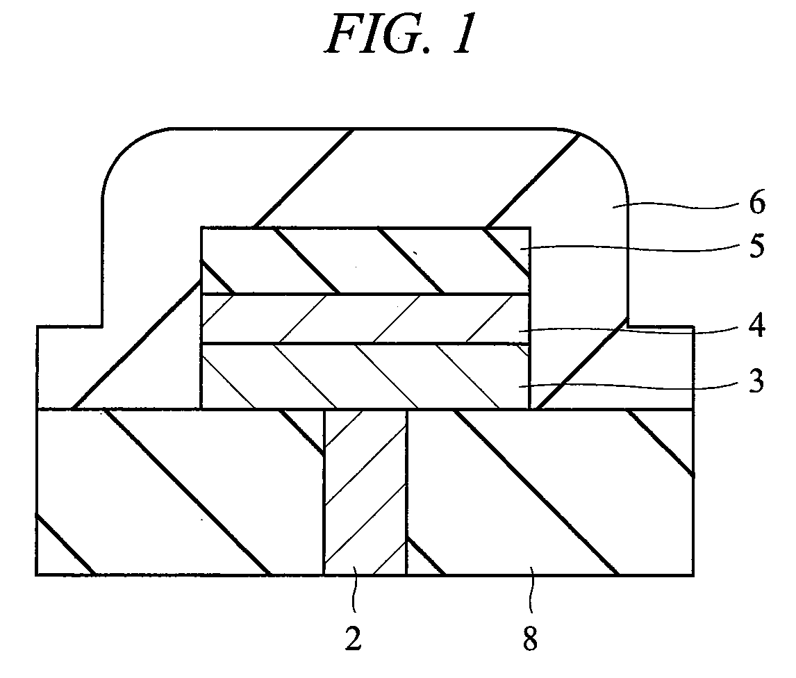
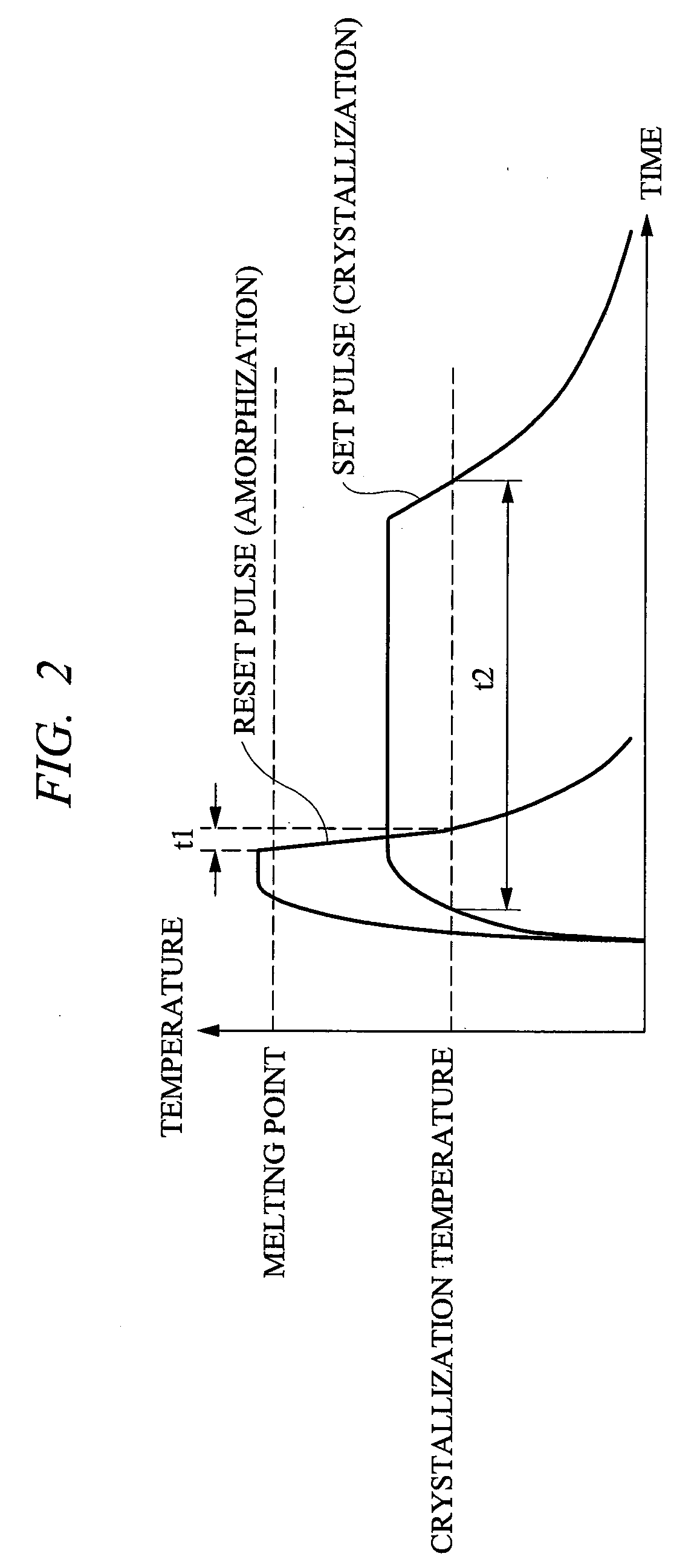
[0046]First, a phase-change memory cell according to the present invention will be described with reference to FIG. 1 and FIG. 2. FIG. 1 is a cross sectional view of main parts schematically showing the phase-change memory cell according to the present invention. FIG. 2 is an explanatory diagram showing current pulse specifications for changing phase states of a chalcogenide.

[0047]The phase-change memory of FIG. 1 comprises: an interlayer dielectric film 8 provided above a select transistor (not illustrated) formed on a main surface of a semiconductor substrate; a plug 2 selectively provided penetrating through the interlayer dielectric film 8 and having an end electrically connected to the select transistor; a chalcogenide material layer 3 electrically connected to the other end of the plug 2 and provided so as to extend on the interlayer dielectric film 8; and a top electrode 4 provided on the chalcogenide material layer 3. Note that, although it will be described later, a fluorin...

second embodiment

[0077]In the above-described first embodiment, the case in which the interlayer dielectric film containing fluorine is formed below the chalcogenide material layer has been described; however, in a present second embodiment, the case in which fluorine is added to the interface between the chalcogenide material layer and the interlayer dielectric film will be described.

[0078]As described above, in the phase-change memory according to the present invention shown in FIG. 1, the adhesive layer 7 formed of a conductive material such as Ti or Al is not provided like shown in above-described FIG. 10 and FIG. 11. The above-described adhesive layer 7 is provided since the conductive materials are readily reacted with the chalcogenide material, the bonding force of the interface is enhanced, and the exfoliation resistance of the chalcogenide material layer 3 is improved. However, as described above, the problems such that a large current is required for phase change and that the additional st...


PUM


Abstract

A semiconductor device having a phase-change memory cell comprises an interlayer dielectric film formed of, for example, SiOF formed on a select transistor formed on a main surface of a semiconductor substrate, a chalcogenide material layer formed of, for example, GeSbTe extending on the interlayer dielectric film, and a top electrode formed on the chalcogenide material layer. A fluorine concentration in an interface between the interlayer dielectric film and the chalcogenide material layer is higher than a fluorine concentration in an interface between the chalcogenide material layer and the top electrode.

Description

TECHNICAL FIELD[0001]The present invention relates to semiconductor devices and a technique of manufacturing the same, and more particularly, it relates to a technique effectively applied to a semiconductor device having a phase-change memory formed by using a phase-change material such as chalcogenide.BACKGROUND ART[0002]In mobile devices represented by mobile phones, semiconductor memories such as DRAM, SRAM, and FLASH memory are used. Each of the memories has advantages and disadvantages, and currently, they are subjected to use depending on the characteristics thereof.[0003]For example, while DRAM has a large capacity, the access speed thereof is low. On the other hand, while the speed of SRAM is high, since many transistors as much as 4 to 6 transistors are required per one cell, it is difficult to increase the degree of integration, and it is not suitable for a large-capacity memory.[0004]Moreover, DRAM and SRAM always require power supply to retain data (volatile). On the oth...

Claims


Application Information

Patent Timeline
Patent Type & Authority Applications(United States)
IPC IPC(8): H01L47/00H01L21/3205
CPCH01L27/2436H01L45/144H01L45/1233H01L45/06Y10S257/903H10B63/30H10N70/231H10N70/826H10N70/8828
Inventor MATSUI, YUICHI
Owner RENESAS ELECTRONICS CORP
Why Eureka
Try Eureka