Power amplifier

a power amplifier and power supply technology, applied in the direction of rf amplifiers, high frequency amplifiers, gain control, etc., can solve the problems of high susceptibility to device variations, low controllability of idle current, and complicated control circuits, so as to improve idle current controllability, stable temperature characteristics, and unsusceptible to device variations

Active Publication Date: 2009-02-26
MURATA MFG CO LTD
View PDF10 Cites 15 Cited by
  • Summary
  • Abstract
  • Description
  • Claims
  • Application Information

AI Technical Summary

Benefits of technology

[0016]The present invention has been achieved to solve the above-described problems and an object of the present invention is to provide a power amplifier having improved idle current controllability, unsusceptibility to device variations and stable temperature characteristics.
[0018]The present invention makes it possible to obtain a power amplifier having improved idle current controllability, unsusceptibility to device variations and stable temperature characteristics.

Problems solved by technology

However, this method requires a complicated control circuit.
However, there are only a small number of documents disclosing a GaAs-HBT power amplifier in which the idle current is controlling in an analog manner.
The power amplifier shown in FIG. 19 has a problem that the control voltage and the idle current are in a nonlinear relationship with each other and, therefore, the controllability of the idle current is low.
The amplifier also has a problem that since the idle current control function and the biasing function are incorporated in one circuit, its susceptibility to device variations is high and it is difficult to make constant the temperature characteristic of the idle current (variation in idle current with temperature with respect to the same control voltage).

Method used


Image

  • Power amplifier
  • Power amplifier
  • Power amplifier

Examples


first embodiment

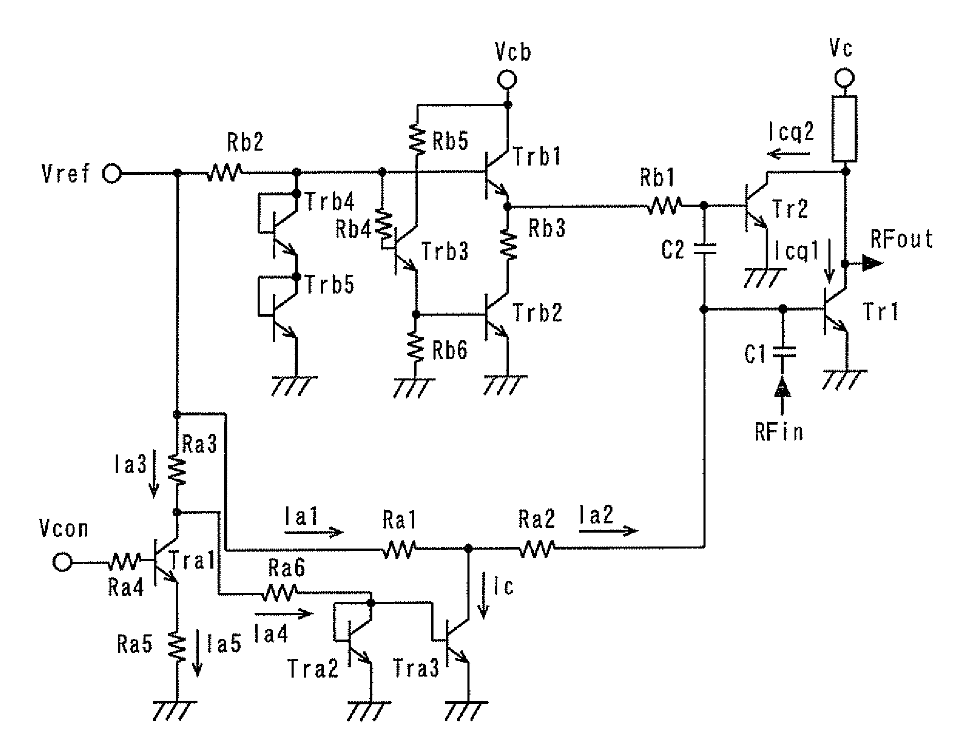
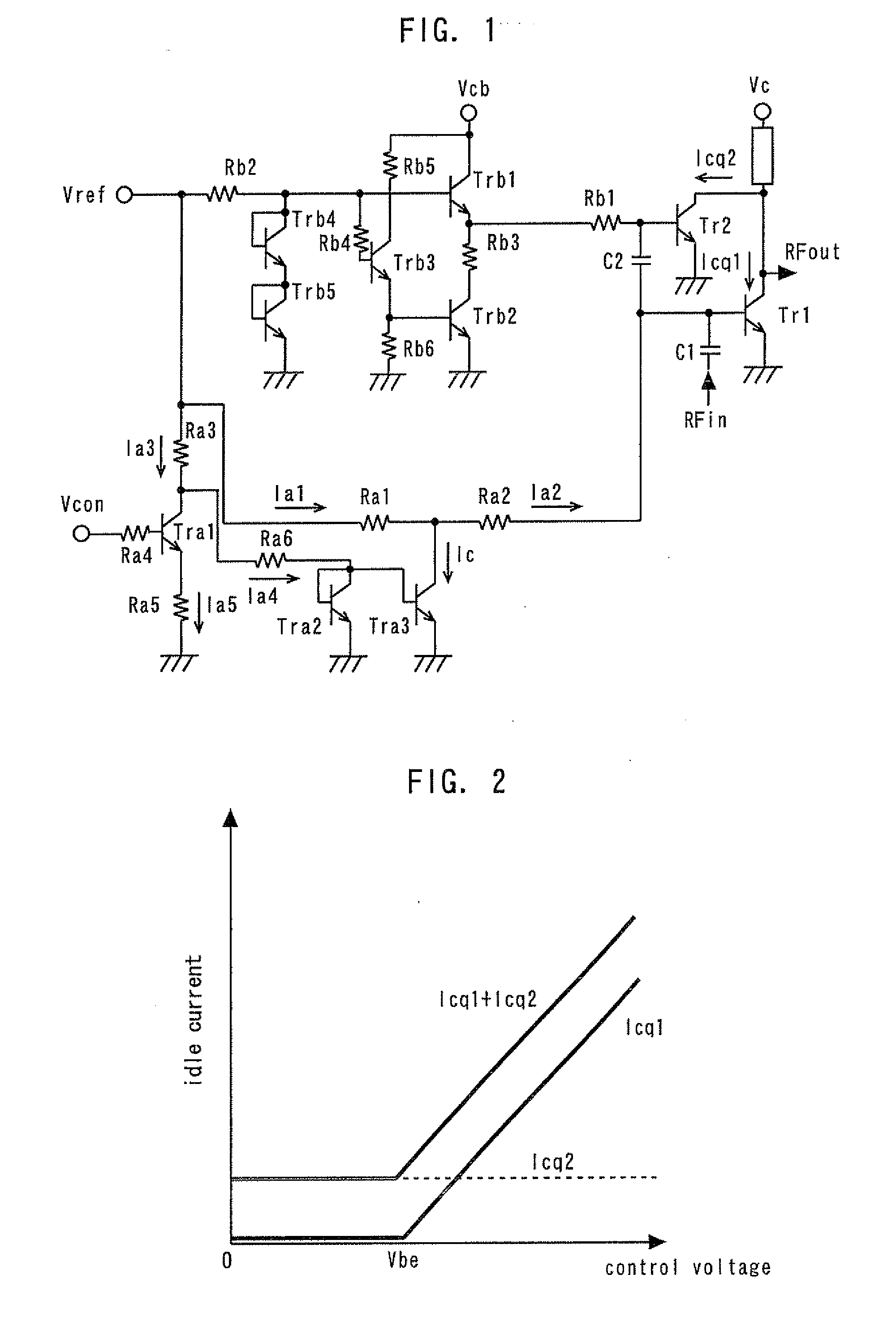
[0039]FIG. 1 is a circuit diagram showing a power amplifier according to a first embodiment of the present invention. Tr1 denotes a first amplifying device; Tr2, a second amplifying device; Vc, a collector power supply terminal of the amplification stage constituted by the first and second amplifying devices Tr1 and Tr2; Vcb, a collector power supply terminal of a bias circuit; Vref, a reference terminal to which a reference voltage (ordinarily 2.8 to 2.9 V) is externally applied; and Vcon, a control terminal to which a control voltage is externally applied. Trb1 to Trb5 and Tra1 to Tra3 denote GaAs-HBTs. Rb1 to RbG and Ra1 to Ra6 denote resistors. An input matching circuit and an output matching circuit are omitted.

[0040]An RF signal input from a terminal RFin is input to the base (input terminal) of the first amplifying device Tr1 via a capacitor C1 of the input matching circuit. The first amplifying device Tr1 amplifies the RF signal and outputs from its collector (output termina...

second embodiment

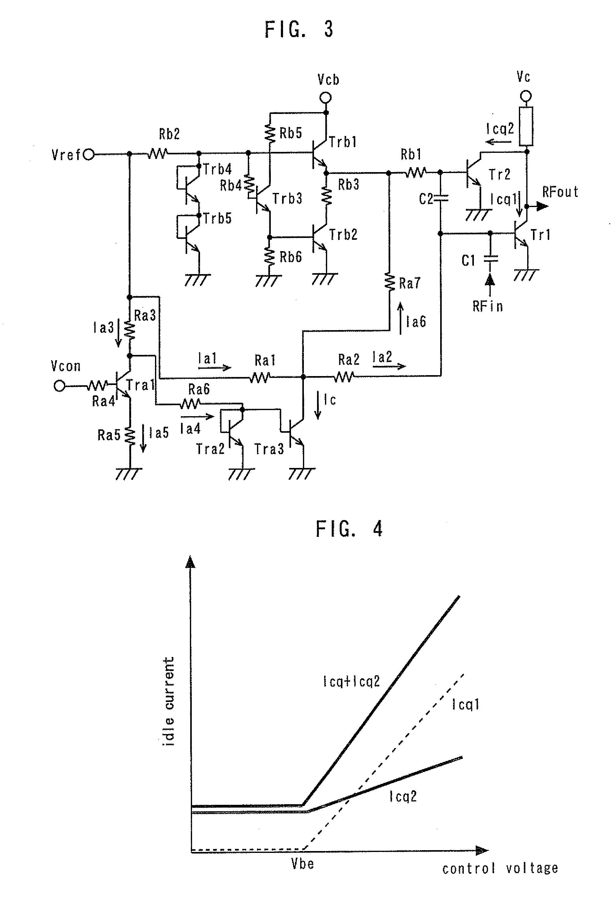
[0051]FIG. 3 is a circuit diagram showing a power amplifier according to a second embodiment of the present invention. A fourth resistor Ra7 is connected between the base (input terminal) of the second amplifying device Tr2 and the connection point between the first and second resistors Ra1 and Ra2. In other respects, the configuration of the second embodiment is the same as that of the first embodiment. This arrangement enables maintaining the control voltage and the idle current in a linear relationship with respect to the second amplifying device Tr2 as well as with respect to the first amplifying device Tr1, as shown in FIG. 4. Thus, the idle current through the second amplifying device Tr2 can be increased during high-output-power operation to obtain an output characteristic with reduced distortion.

third embodiment

[0052]FIG. 5 is a circuit diagram showing a power amplifier according to a third embodiment of the present invention. The base and the collector of the second transistor Tra4 are connected to the reference terminal Vref. A fifth resistor Ra8 is connected between the emitter of the second transistor Tra4 and the connection point between the first and second resistors Ra1 and Ra2. In other respects, the configuration of the third embodiment is the same as that of the first embodiment.

[0053]In the first embodiment, if the control voltage is constant, the idle current Icq1 through the first amplifying device Tr1 is constant with respect to varying temperature. If the idle current is constant, the gain of the HBT power amplifier decreases with increase in temperature. Thus, there has been a problem that the gain of the power amplifier decreases with increase in temperature. In the third embodiment of the present invention, the idle current Icq1 through the first amplifying device Tr1 can...


PUM


Abstract

An emitter follower circuit applies to an input terminal of a second amplifying device a voltage according to a reference voltage applied to a reference terminals. First and second resistors are connected in series between the reference terminal and an input terminal of a first amplifying device. The collector of a first transistor is connected to the reference terminal, and a control voltage is applied to the base of the first transistor. A third resistor is connected between the emitter of the first transistor and a grounding point. A current mirror circuit draws a current proportional to a current input from the collector of the first transistor from a connection point of the first and second resistors.

Description

BACKGROUND OF THE INVENTION[0001]1. Field of the Invention[0002]The present invention relates to a power amplifier having improved idle current controllability, reduced susceptibility to device variations and stable temperature characteristics.[0003]2. Background Art[0004]Power amplifiers using GaAs heterojunction bipolar transistors (GaAs-HBT) are presently used widely as power amplifiers for use in portable telephone in CDMA and other systems. FIG. 13 is a circuit diagram showing a conventional GaAs-HBT power amplifier. The area in the dotted frame in FIG. 13 corresponds to a GaAs chip. Circuit elements in the other area are formed of chip parts and conductor lines on a module substrate.[0005]In FIG. 13, reference characters Tr1 and Tr2 denote a preceding-stage amplifying device and a following-stage amplifying device, respectively. Bias1 denotes a preceding-stage bias circuit for driving the preceding-stage amplifying device, and Bias2 denotes a following-stage bias circuit for d...

Claims


Application Information

Patent Timeline
Patent Type & Authority Applications(United States)
IPC IPC(8): H03G3/10
CPCH03F1/302H03F3/19H03G1/0035H03F2200/447H03F2200/451H03F2200/18
Inventor YAMAMOTO, KAZUYAMIYASHITA, MIYO
Owner MURATA MFG CO LTD
Why Eureka
Try Eureka