Semiconductor device with a u-shape drift region

a technology of u-shape and drift region, which is applied in the direction of semiconductor devices, basic electric elements, electrical apparatus, etc., can solve the problems of large area, more complex process, and high manufacturing cost, and achieve low manufacturing cost, simple device processing, and the effect of almost eliminating the tail of the turn-o

Inactive Publication Date: 2009-03-05
UNIV OF ELECTRONICS SCI & TECH OF CHINA
View PDF7 Cites 17 Cited by
  • Summary
  • Abstract
  • Description
  • Claims
  • Application Information

AI Technical Summary

Benefits of technology

[0026]One advantage of the present invention is to implement two device feature regions within one surface of a substrate, instead of implement any device feature region on the opposite surface (the bottom) of a substrate, which leads to a simple processing of devices and a low fabrication cost. Another advantage of the present invention is to implement an IGBT with a second gate assisting in the turn-off process, wherein the minority carrier injection ratio can be controlled and thus the tail of turn-off can be almost eliminated. Still another advantage of the present invention is an implementation of a power transmission gate with an n-MOST and a p-MOST by integration in one area instead of in two different areas. A further advantage of the present invention is to fabricate low voltage devices in power (or high-voltage) integrated circuit without additional dielectric isolation or junction isolation.

Problems solved by technology

It is noticed the drift region in above devices is doped oppositely to the doping type of the substrate, leading to a more complex process.
Furthermore, the device feature region, including the source region, the source-body region and part of the gate region is formed outside of the U-shape drift region, causing a large area.
Although trench etching is a mature process in modern technology of micro-electronics, the method of forming the gate in Baliga, B. J., U.S. Pat. No. 5,434,435 (1995) still makes the process more complex.
In addition, another direct wafer bonding or epitaxy should be conducted for growing the intermediate layer for isolation, leading to a higher cost.
Obviously, the implementation of the latter device feature region causes a more complex process and a higher fabrication cost.
Even such a trade-off is optimized, it is still not able to eliminate the injection of the minorities during the turn-off process entirely.

Method used


Image

  • Semiconductor device with a u-shape drift region
  • Semiconductor device with a u-shape drift region
  • Semiconductor device with a u-shape drift region

Examples


Embodiment Construction

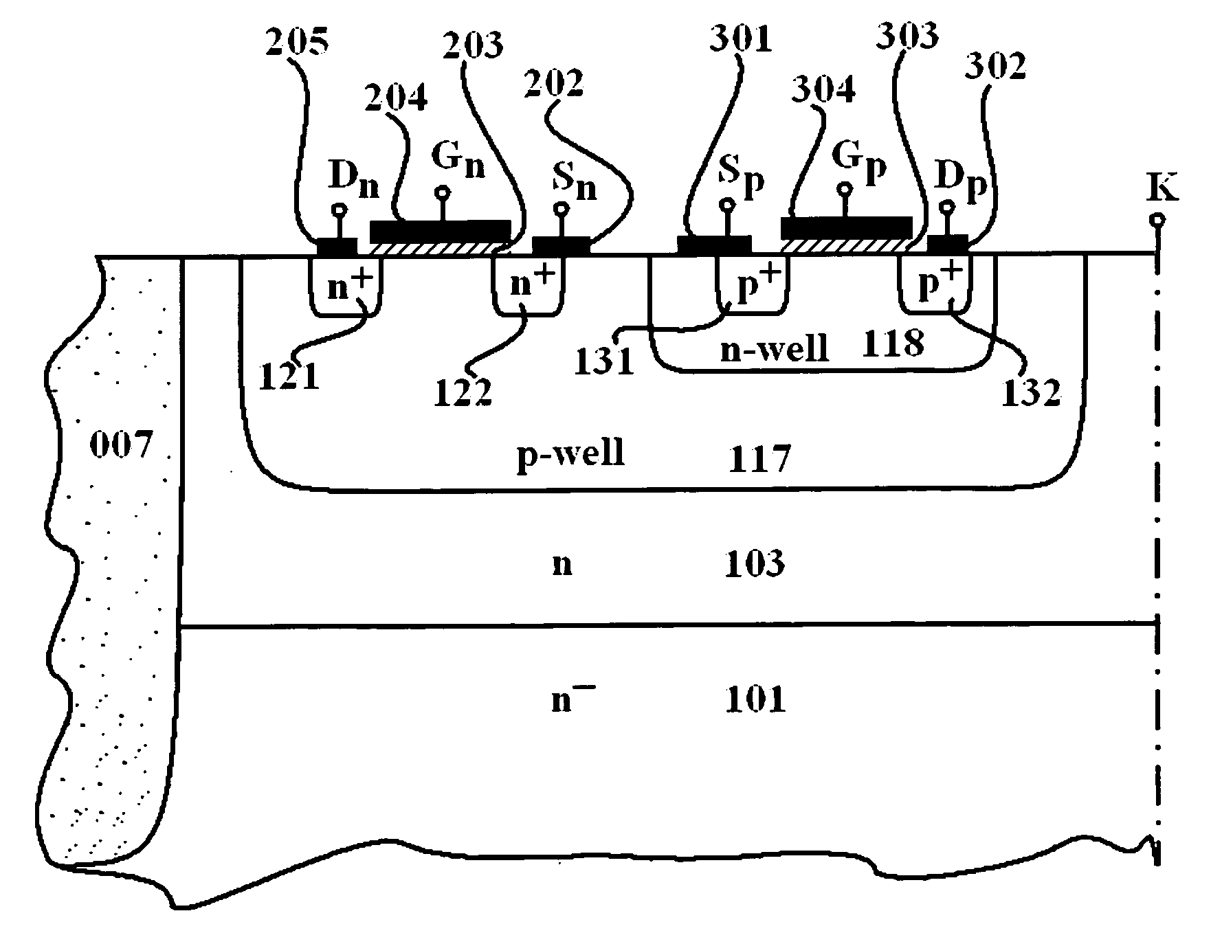
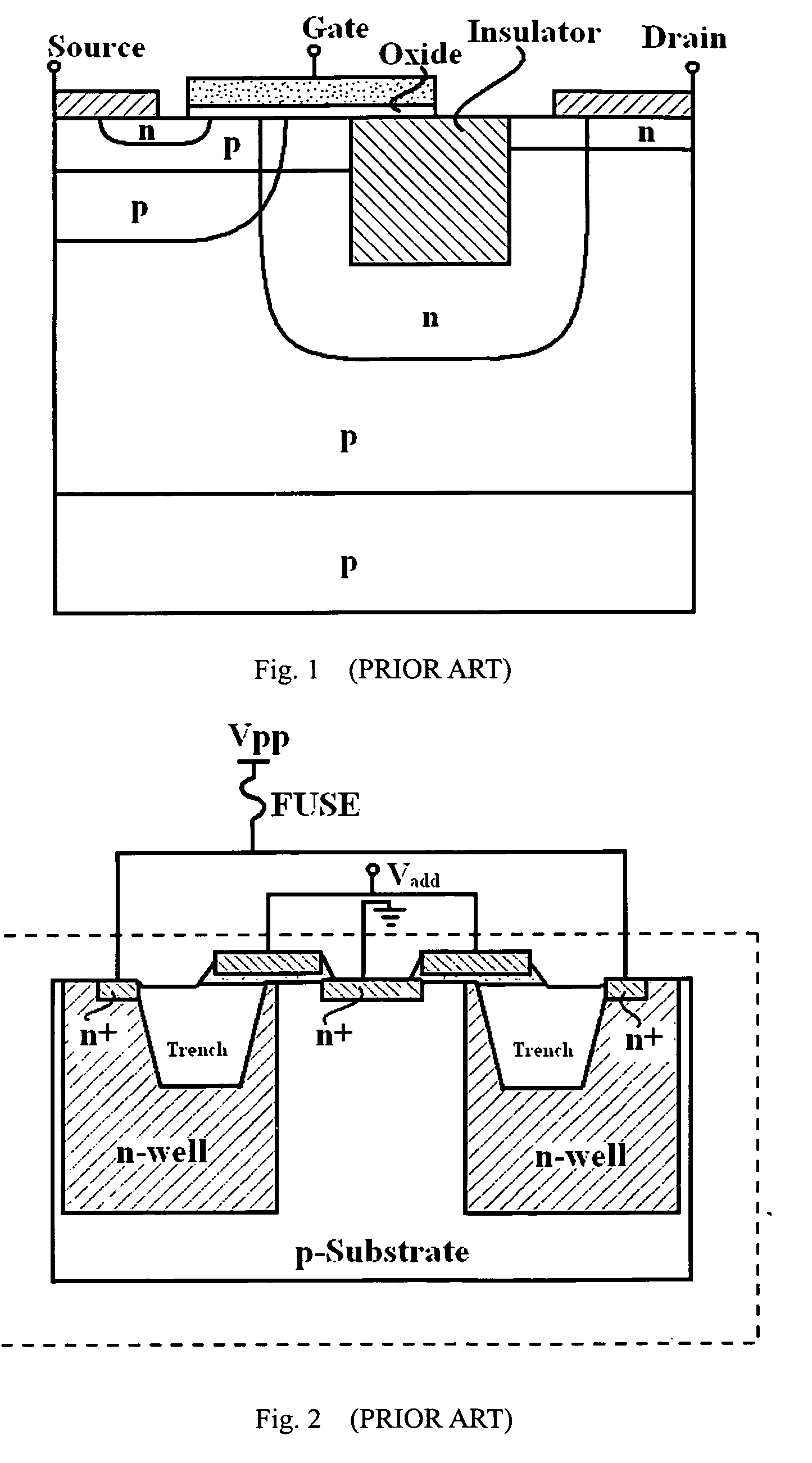
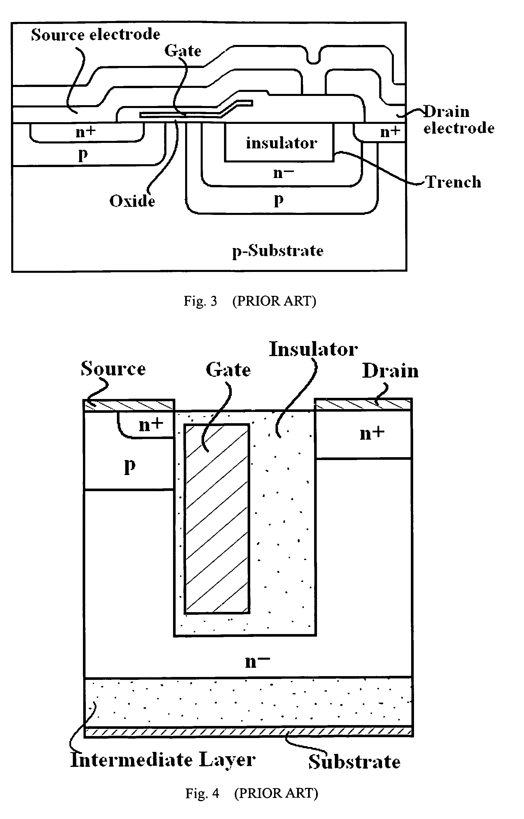
[0054]Due to that in most of devices, the sustaining of a reverse biased voltage can be explained based on a p-n junction, we start from an explanation of the drift region of this invention from a p-n junction diode under a reverse bias. FIG. 5 shows a cross-sectional view of a device structure 100 in the present invention. The dash-dotted lines represent the boundaries of a cell of the device. In this figure, the n-region, 101, is a U-shape drift region. A trench 010 is formed inside the U-shape region and filled with an insulator material 007 represented by dotted area in the figure. The portions at the top of the semiconductor of the two sides of the trench are the two device feature regions, where the first device feature region is on the first side and the second device feature region is on the second side. The bold line 001 at the left side of the U-region represents the conductor for forming the anode, A, which is connected to the p+-region 102 (the second type of conductivit...


PUM


Abstract

A semiconductor device with a U-shape drift region comprises a semiconductor substrate of a first conductivity type, a trench filled with an insulator material formed in a portion of a first main surface of the substrate, a cell of the device including the trench and semiconductor region surrounding the trench. The semiconductor device has at least one cell. Two device-feature regions are formed beneath the first main surface of the substrate, the first one is located at one side and the second one is located at the other side of the trench. At least a region of a second conductivity type and/or a region of metal is formed in the first device feature region and is connected to a first electrode. At least a region of a first conductivity type and/or a region of metal is formed in the second device feature region and is connected to a second electrode. Based on this invention, semiconductor devices, especially, an IGBT without tail during turning-off can be fabricated with a simple process at a low cost.

Description

CROSS-REFERENCES TO RELATED APPLICATIONS[0001]This application claims priority to Chinese Patent Application No. 200710145552.1, filed Aug. 28, 2007, the contents of which are hereby incorporated by reference in its entirety.FIELD OF THE INVENTION[0002]This invention is related to semiconductor devices, and particularly related to high-voltage devices and / or power devices, which can be discrete ones and can also be implemented in power integrated circuits.BACKGROUND OF THE INVENTION[0003]In a conventional vertical high-voltage device, a low-resistivity substrate is normally used to reduce the on-resistance. On the low-resistivity substrate, a high resistivity layer is grown as the drift region (also called as the voltage sustaining layer) by epitaxy or direct wafer bonding. In some vertical devices, there are more epi-layers that need to grow. For instance, in a non-punch-through IGBT, an n+-type (or a p+-type) thin epi-layer is first grown on a p+(or n+)-substrate, and then a thick...

Claims


Application Information

Patent Timeline
Patent Type & Authority Applications(United States)
IPC IPC(8): H01L29/78H01L29/872H01L29/772
CPCH01L27/0925H01L27/0927H01L27/0928H01L29/063H01L29/0634H01L29/872H01L29/0653H01L29/0692H01L29/7325H01L29/7809H01L29/861H01L29/0649
Inventor CHEN, XINGBI
Owner UNIV OF ELECTRONICS SCI & TECH OF CHINA
Why Eureka
Try Eureka