Edge bead removal process with ecmp technology

a technology of ecmp and conductive layer, which is applied in the direction of manufacturing tools, electric circuits, electric circuits, etc., can solve the problems of short circuit, delamination of copper layer, other problems, and achieve the effect of only removing excess copper

Inactive Publication Date: 2009-03-05
APPLIED MATERIALS INC
View PDF2 Cites 3 Cited by
  • Summary
  • Abstract
  • Description
  • Claims
  • Application Information

AI Technical Summary

Problems solved by technology

The excess copper on the face can cause problems such as shorts in the circuit.
Additionally, the excess copper extending onto the edge of the substrate can lead to delamination of the copper layer and other problems even if the edge portion is part of an unusable section of the substrate.
However, ECMP effectively only removes the excess copper on the face of the substrate and not the edge of the substrate since the polishing material does not contact the edge.
Thus, the additional EBR step in the manufacture of the integrated circuit increases costs by slowing throughput, increasing the overall complexity of the system used for deposition, and requiring use of additional consumable material.

Method used


Image

  • Edge bead removal process with ecmp technology
  • Edge bead removal process with ecmp technology
  • Edge bead removal process with ecmp technology

Examples


Embodiment Construction

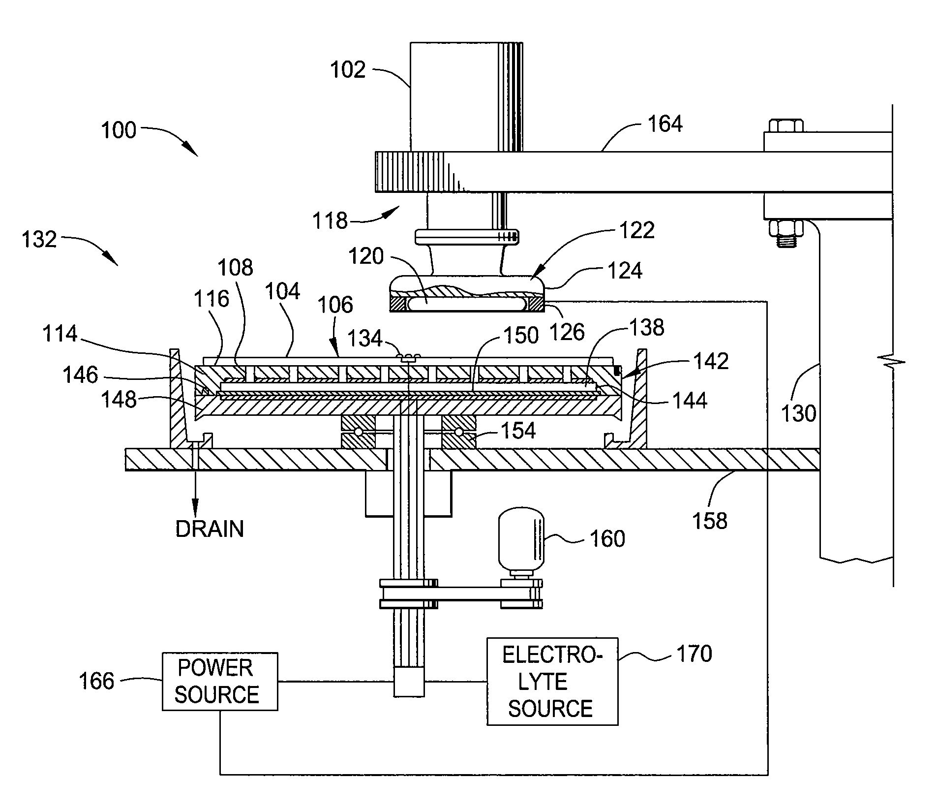
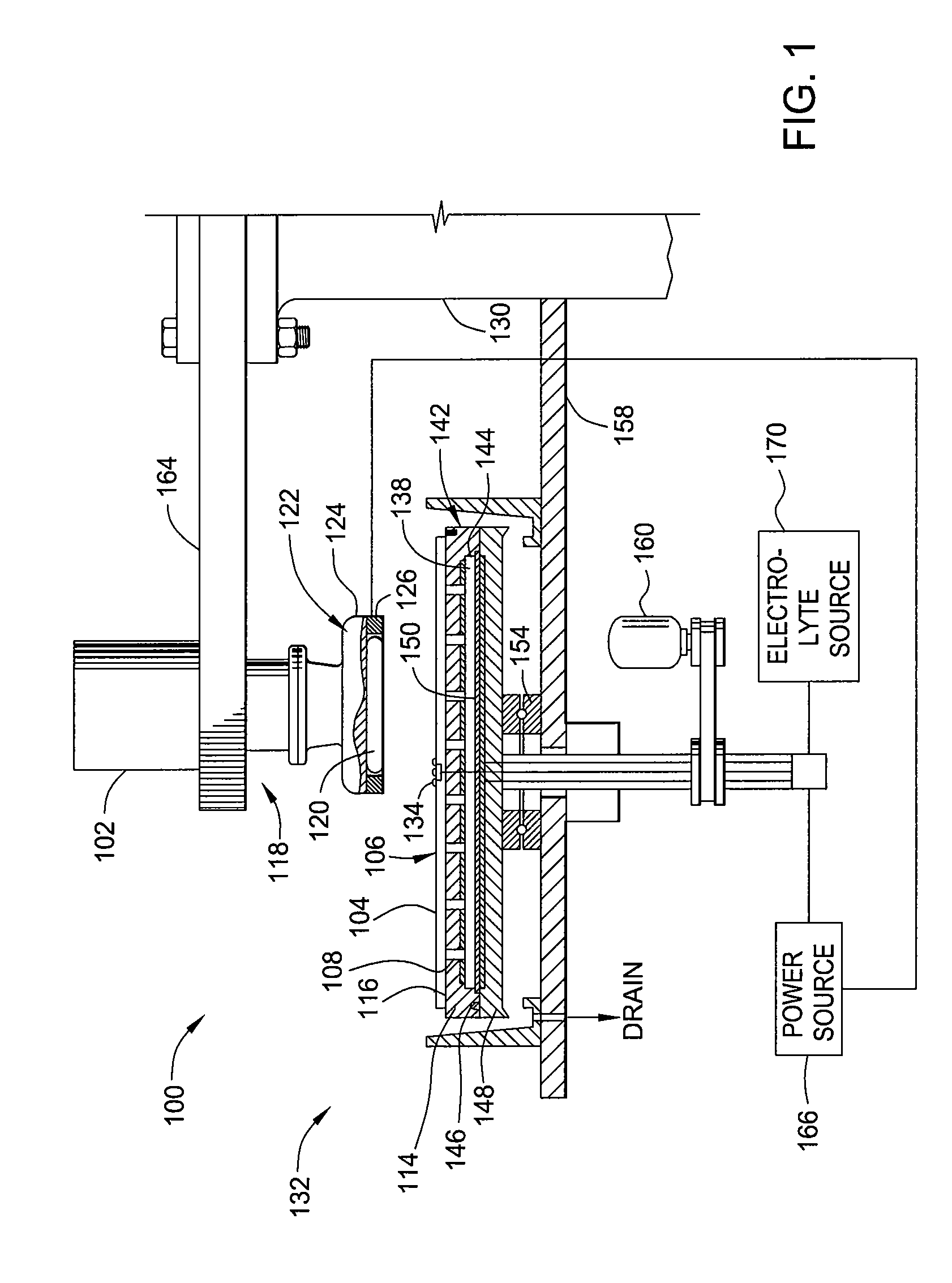
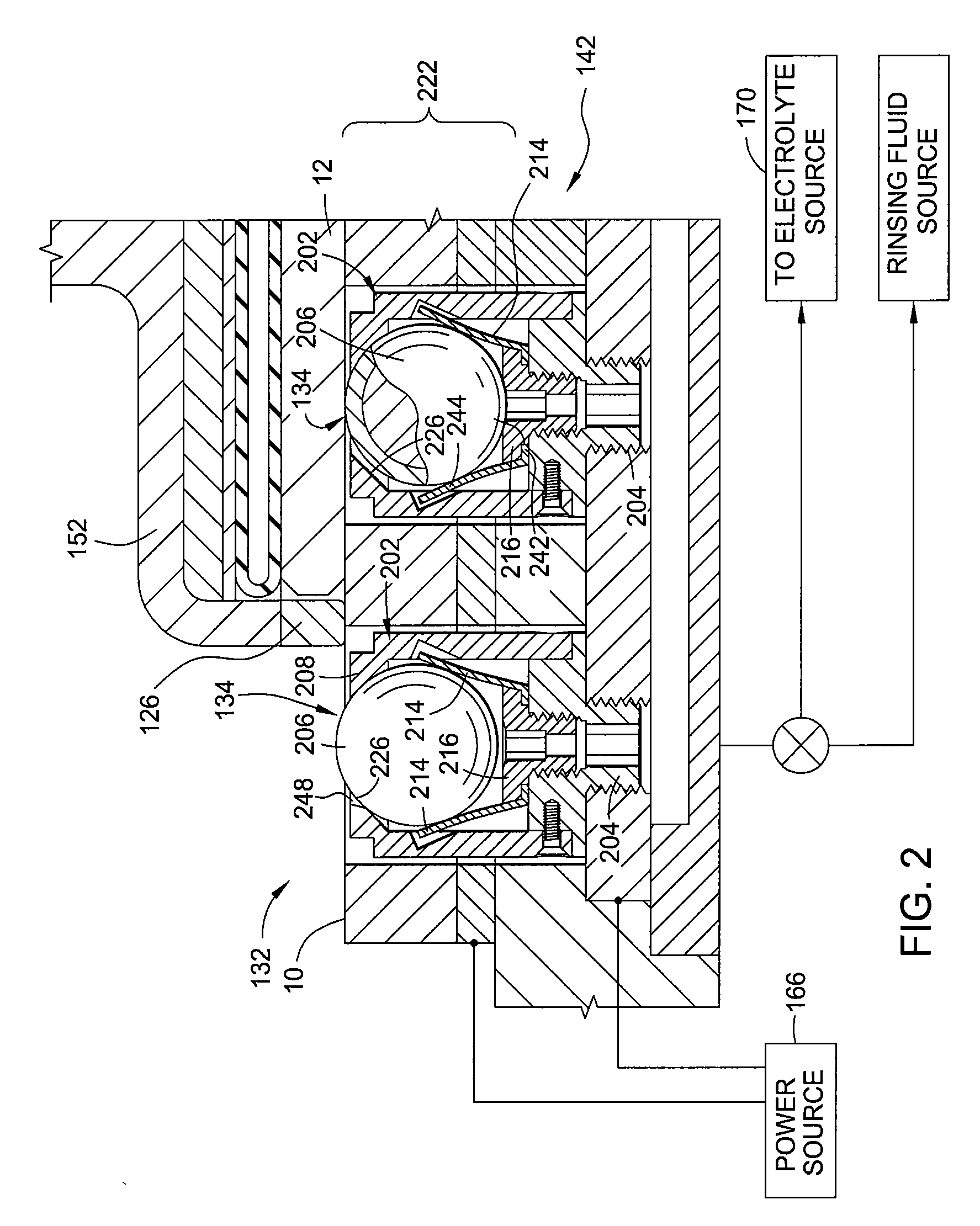
[0018]Embodiments of the invention as recited in the claims generally relate to edge bead removal (EBR) from a substrate during an electropolishing process. The edge bead removal may occur simultaneously during electrochemical mechanical polishing (Ecmp) of the surface of the substrate.

[0019]As used herein, the term “electrochemical mechanical polishing” (Ecmp) generally refers to planarizing a substrate by the application of electrochemical activity, mechanical activity, abrading, and chemical activity to remove material from a substrate surface.

[0020]As used herein, the term “electro polishing” generally refers to planarizing a substrate by the application of electrochemical activity without abrasion between the surface to be planarized and the polishing pad.

[0021]As used herein, the term “substrate” generally refers to any substrate or material surface formed on a substrate upon which film processing is performed, such as silicon wafers used in semiconductor processing. For examp...


PUM

PropertyMeasurementUnit
voltageaaaaaaaaaa
voltageaaaaaaaaaa
voltageaaaaaaaaaa

Abstract

A method and apparatus for the removal of a deposited conductive layer along an edge of a substrate using a power ring configured to electro polish an edge of the substrate are provided. The electro polishing of the substrate edge may occur simultaneously with the electrochemical mechanical processing of a substrate face. In certain embodiments a method of electrochemically polishing a substrate having a conductive material disposed thereon is provided. A substrate is coupled with a carrier head comprising a power ring which surrounds an edge of the substrate, wherein the edge of the substrate includes the conductive material. A polishing pad is contacted with a face of the substrate. A first voltage is applied to the power ring to remove conductive material from the edge of the substrate. A second voltage different from the first voltage is applied to the polishing pad to remove a portion of the conductive material from the face of the substrate.

Description

BACKGROUND OF THE INVENTION[0001]1. Field of the Invention[0002]Embodiments of the present invention as recited in the claims generally relate to removal of a deposited conductive layer from a substrate. More particularly, embodiments of the invention relate to electro polishing the edge of a substrate during electrochemical mechanical polishing of the face of the substrate.[0003]2. Description of the Related Art[0004]In the fabrication of integrated circuits and other electronic devices, deposition of a conductive layer on a substrate, such as a copper layer used to fill features formed within a dielectric material, results in excess copper deposited on a face of the substrate and a peripheral edge of the substrate that wraps onto the face. The excess copper on the face can cause problems such as shorts in the circuit. Additionally, the excess copper extending onto the edge of the substrate can lead to delamination of the copper layer and other problems even if the edge portion is ...

Claims


Application Information

Patent Timeline
Patent Type & Authority Applications(United States)
IPC IPC(8): H01L21/3063
CPCH01L21/3063H01L21/02087
Inventor DUBOUST, ALAINSALAS-VERNIS, JOSEMANENS, ANTOINE P.
Owner APPLIED MATERIALS INC
Why Eureka
Try Eureka