Input circuitry for transistor power amplifier and method for designing such circuitry

a technology of input circuitry and power amplifier, which is applied in the direction of amplifiers, amplifiers with semiconductor devices only, amplifiers, etc., can solve the problems of significant degradation of amplifier efficiency at high input power levels using fixed input impedance networks, poor performance under high drive power, and reduced efficiency, etc. , to achieve the effect of low signal power levels, poor performance and good stability

Active Publication Date: 2009-03-12
RAYTHEON CO
View PDF4 Cites 16 Cited by
  • Summary
  • Abstract
  • Description
  • Claims
  • Application Information

AI Technical Summary

Benefits of technology

[0019]The invention thus incorporates an input signal power level dependent element (i.e., a configurable input matching network). First, an optimal small signal input matching network configuration is attached to the GaN transistor. This provides good stability, return loss, and power transfer from an RF input to the amplifying transistor at low drive powers (i.e., low signal power levels), but at the expense of poor performance under high drive powers (i.e., high signal power levels). The reconfigured input matching network is then used to rotate the phase angle (i.e., match), only under high input signal power levels, to that what is optimal for realizing peak performance without soft compression. For example, at S-band for a 2.5 mm periphery transistor, this input matching network will only have to rotate the original phase angle by 10 degree clockwise on the Smith Chart. The reconfigured input matching network is disconnected from

Problems solved by technology

Because of soft compression the non-ideal FET will require a higher input drive level to obtain power saturation of the device and the amplifier designed with such FETs will also require a higher drive than normal.
Furthermore, a 2-stage GaN amplifier will require a conservative choice of the FET ratio between stages, thereby contributing to reduced efficiency.
Applicants have discovered that there is significant degradation to amplifier efficien

Method used


Image

  • Input circuitry for transistor power amplifier and method for designing such circuitry
  • Input circuitry for transistor power amplifier and method for designing such circuitry
  • Input circuitry for transistor power amplifier and method for designing such circuitry

Examples


Embodiment Construction

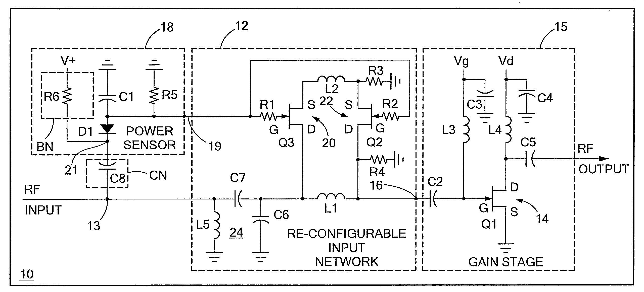
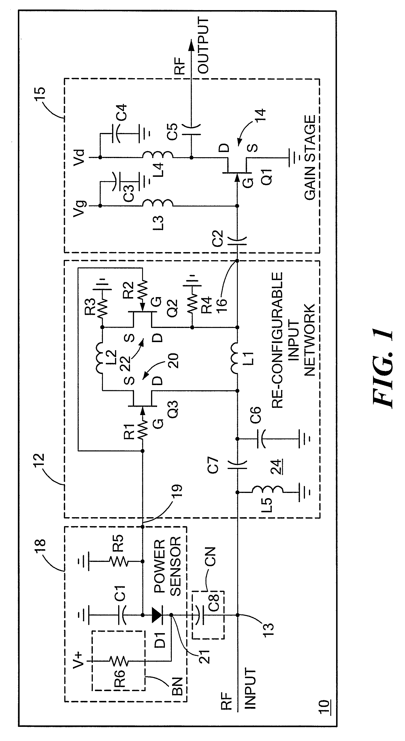
[0037]Referring now to FIG. 1, a power amplifier circuit 10 is shown to include: an input matching network 12 having an input terminal 13 for coupling to an RF input signal; an output stage 15 having a transistor14, here a gallium arsenide (GaN) field effect transistor (FET) with a field plate, coupled to an output 16 of the input matching network 12. As will be described in more detail below, the input matching network 12 is configurable as a function of the power level, of the input signal. More particularly, the input matching network 12 is configured to have a first input impedance when such input matching network 12 is fed with the input signal having a relatively low power level and is configured to have a different input impedance from the first input impedance when such input matching network 12 is an input signal having a relatively high power level.

[0038]More particularly, the amplifier circuit 10 includes a power level sensing circuit 18 connected to input 13 and thus is ...


PUM


Abstract

A circuit having: an input matching network; a transistor coupled to an output of the input matching network; and wherein the input matching network has a first input impedance when such input matching network is fed with an input signal having a relatively low power level and wherein the input matching network has an input impedance different from the first input impedance when such input matching network is fed with an input signal having a relatively high power level.

Description

TECHNICAL FIELD[0001]This invention relates generally to transistor power amplifiers and more particularly to input circuitry for such transistor power amplifiers.BACKGROUND AND SUMMARY[0002]As is known in the art, it is frequently desirable to operate the amplifier linearly and with high efficiency over a wide range of input power levels. In order to design such a power amplifier, a fixed input impedance network is designed which compromises between performance at high input power levels and low input power levels.[0003]As is also known in the art, Gallium Nitride (GaN) transistors are high band gap semiconductor devices that operate at high voltages (typically, 20 to 50V) and high current densities (up to 1.5 A / mm). The devices have been demonstrated to produce 6 W / mm for large periphery devices (over 2 mm) over the frequency range from 2 to 20 GHz. At still higher frequencies up to 40 GHz the transistors have been shown to produce up to 4 W / mm of output power.[0004]One type of Ga...

Claims


Application Information

Patent Timeline
IPC IPC(8): H03H7/38
CPCH03F1/565H03F3/1935H03F2200/222H03F2200/228H03H7/38H03F2200/252H03F2200/451H03F2200/99H03F2200/249
Inventor WHELAN, COLIN S.TREMBLAY, JOHN C.
Owner RAYTHEON CO
Why Eureka
Try Eureka