Display device and method for manufacturing the same

a technology of display device and manufacturing method, which is applied in the direction of identification means, instruments, optics, etc., can solve the problems of difficult electrical connection of thin film circuits which are transferred, limit the high performance of display device, etc., and achieve the improvement of the aperture ratio of a pixel, the effect of high field-effect transistor performance and reduced cos

Inactive Publication Date: 2009-03-26
SEMICON ENERGY LAB CO LTD
View PDF40 Cites 98 Cited by
  • Summary
  • Abstract
  • Description
  • Claims
  • Application Information

AI Technical Summary

Benefits of technology

[0028]A semiconductor layer which forms a field-effect transistor is provided by being separated from a semiconductor substrate, so that high performance of the field-effect transistor which forms a pixel of a display device can be realized. In addition, the field-effect transistors in the pixel can be provided with a stacked-layer structure. Therefore, a display device can be provided, which can achieve improvement in an aperture ratio of a pixel, which has been reduced due to increase in the number of field-effect transistors, and reduction in the area of the field-effect transistor which occupies a pixel, without depending on a microfabrication technique of the field-effect transistors, even when the number of field-effect transistors in the pixel is increased.

Problems solved by technology

However, there is limitation on high performance of a display device with dependence only on a microfabrication technique of the field-effect transistor which forms a pixel of a display device.
However, it is difficult to electrically connect thin film circuits which are transferred after separation to each other, which is not preferable in terms of mass productivity.

Method used


Image

  • Display device and method for manufacturing the same
  • Display device and method for manufacturing the same
  • Display device and method for manufacturing the same

Examples


embodiment mode 1

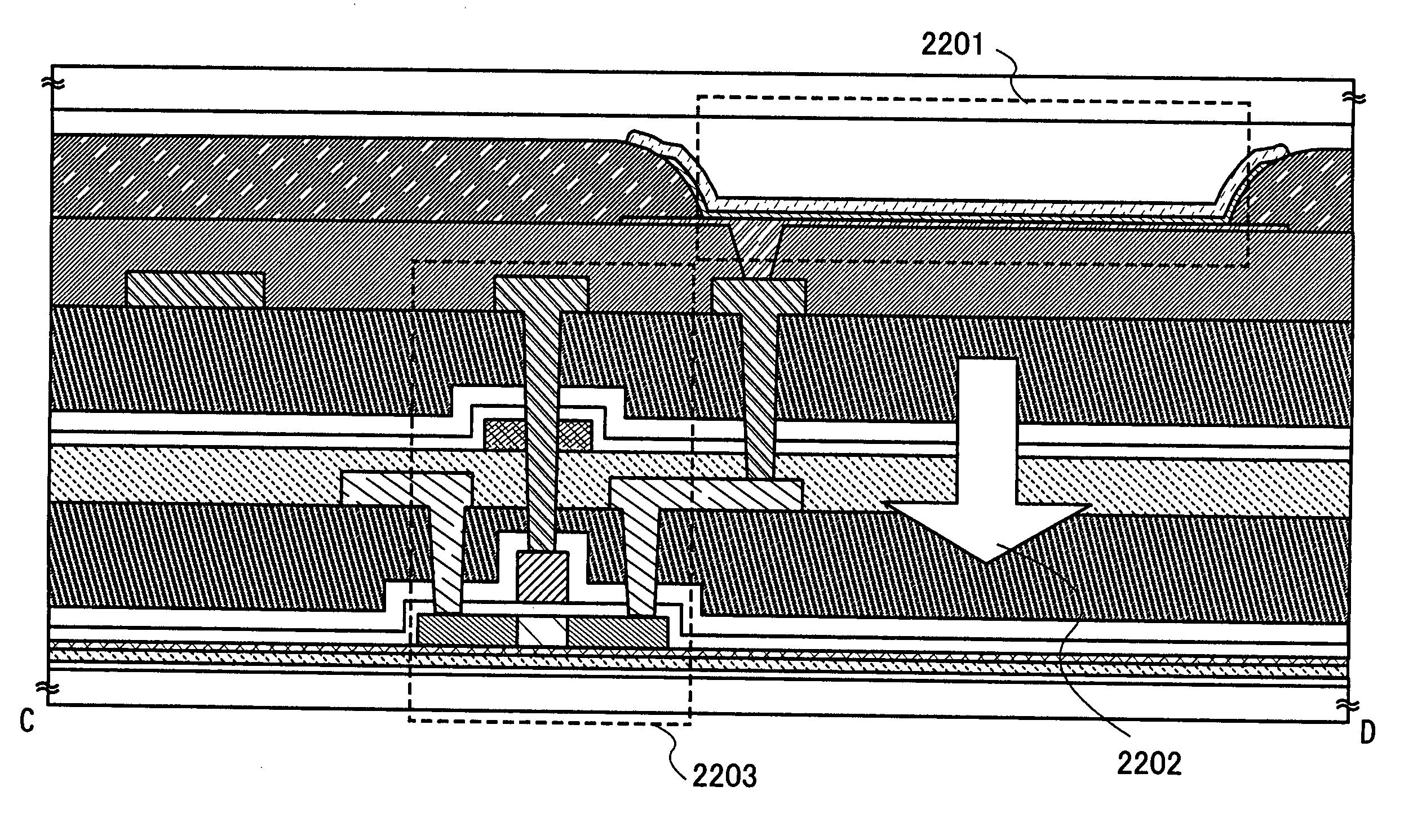
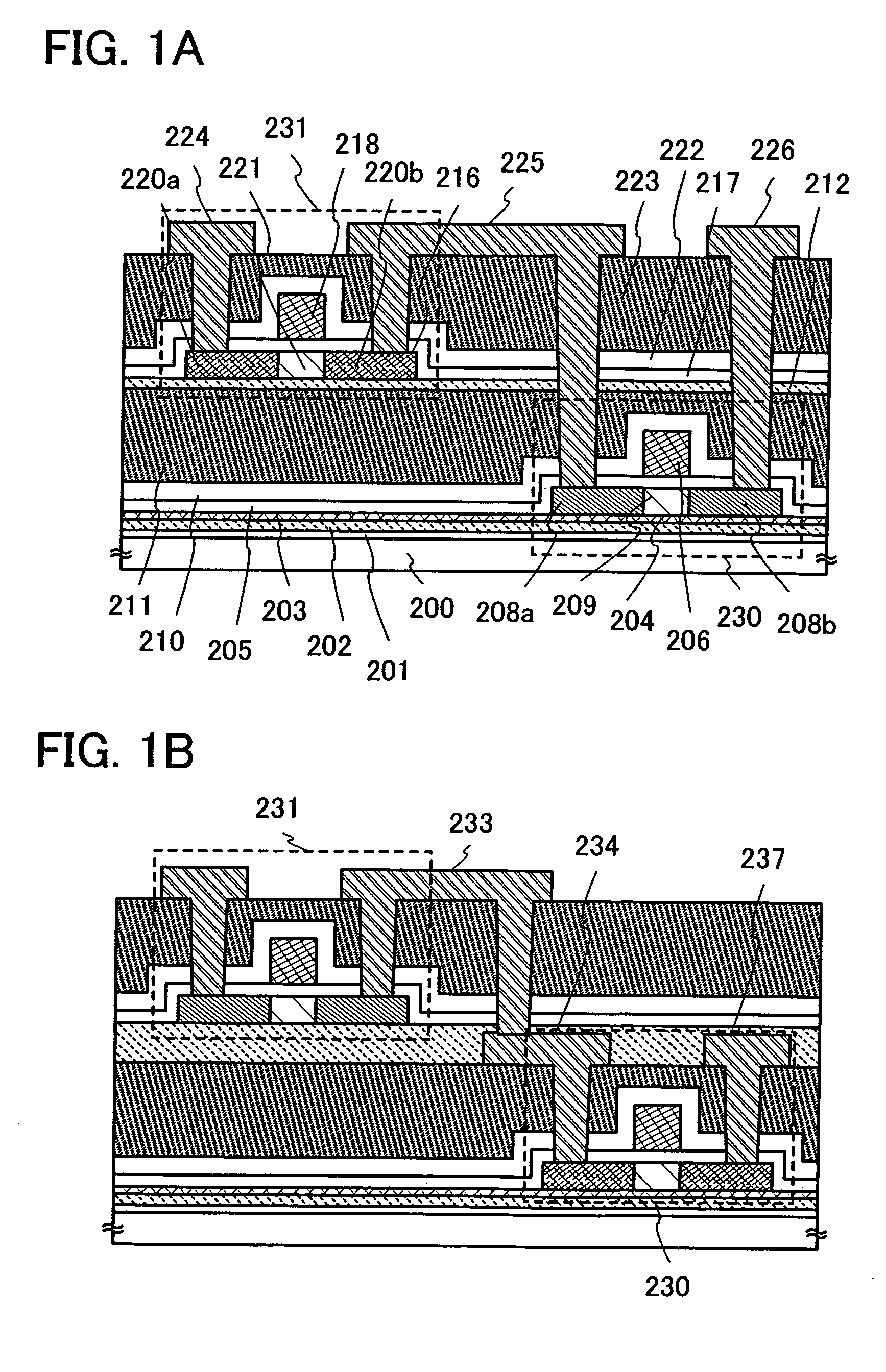
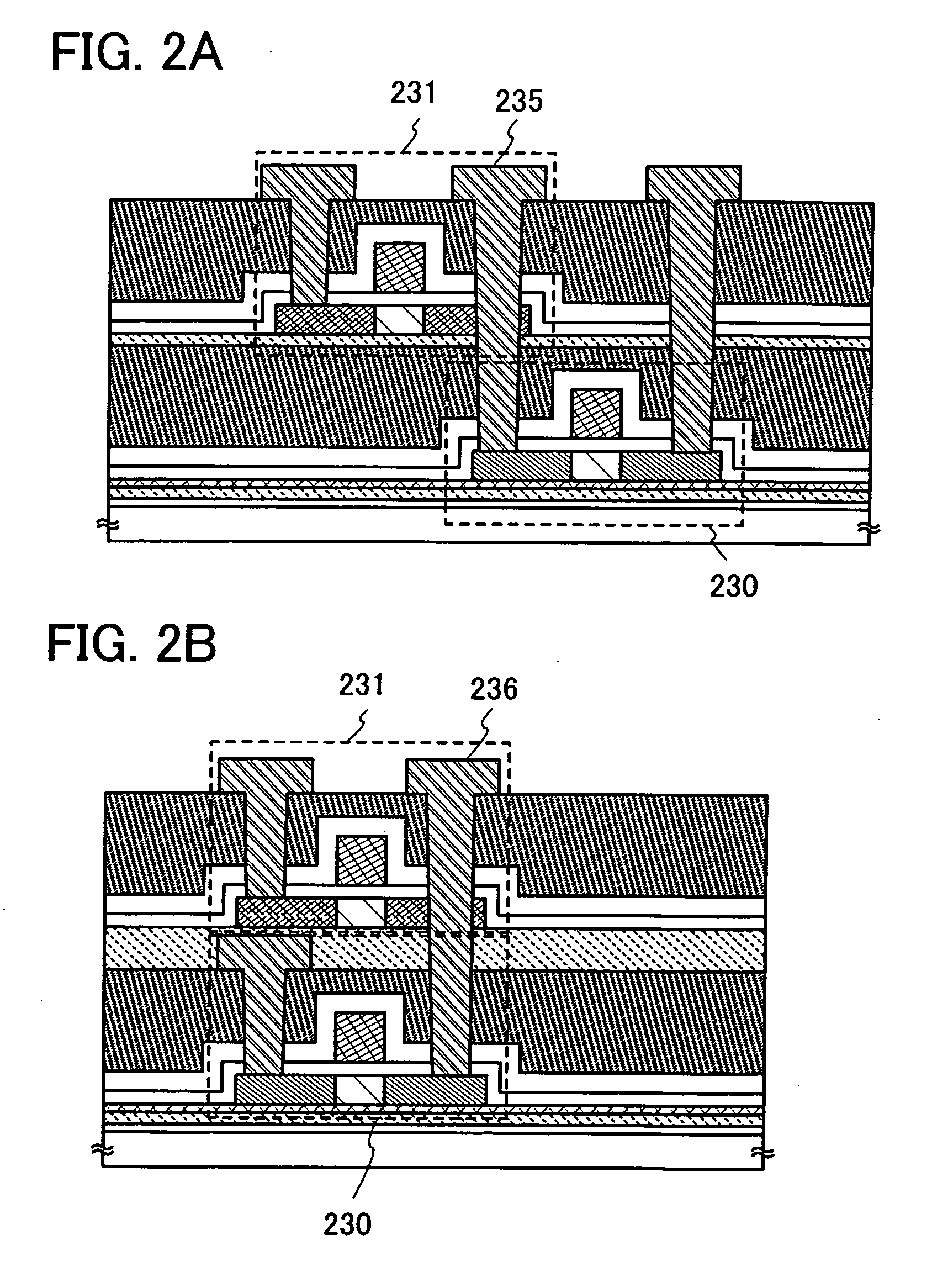
[0053]A method for manufacturing a display device of the present invention is described with reference to FIGS. 1A and 1B, FIGS. 2A and 2B, FIGS. 3A to 3D, FIGS. 4A to 4D, FIGS. 5A to 5F, and FIGS. 6A to 6C. This embodiment mode will describe a structure of a pixel provided with a field-effect transistor as an example of a display device. In particular, this embodiment mode will describe a method for electrically connecting field-effect transistors which are formed over different planes with reference to cross-sectional views.

[0054]In this embodiment mode, a field-effect transistor having a semiconductor layer which is separated from a semiconductor substrate and is bonded to a supporting substrate having an insulating surface (or also referred to as a substrate having an insulating surface), a planarization layer, and another field-effect transistor are stacked. It is preferable that a single crystal semiconductor substrate be used as the semiconductor substrate and a single crysta...

embodiment mode 2

[0168]This embodiment mode describes an example in which steps of separating a semiconductor layer from the semiconductor substrate and bonding the semiconductor layer to a supporting substrate are different from steps in Embodiment Mode 1. Therefore, repetitive description of the same portion or a portion having a similar function to the portions in Embodiment Mode 1 is omitted.

[0169]According to this embodiment mode, when a semiconductor layer is transferred from a semiconductor substrate, the semiconductor substrate is etched selectively (this step is also referred to as groove processing), and a plurality of semiconductor layers divided such that they have the size of semiconductor elements to be manufactured are transferred to a supporting substrate. Thus, a plurality of island-like semiconductor layers can be formed over the supporting substrate. Since the semiconductor layers which are processed into an element size in advance are transferred, transfer to the supporting subst...

embodiment mode 3

[0188]This embodiment mode describes an example in which steps of separating a semiconductor layer from the semiconductor substrate and bonding the semiconductor layer to a supporting substrate are different from steps in Embodiment Mode 1. Therefore, repetitive description of the same portion or a portion having a similar function to the portions in Embodiment Mode 1 is omitted.

[0189]This embodiment mode describes an example in which after a semiconductor layer is separated from a semiconductor substrate, the semiconductor layer is bonded to a supporting substrate.

[0190]As described in Embodiment Mode 2 with reference to FIGS. 7A to 7E, the embrittlement layer is formed in the semiconductor substrate and a groove is formed. Groove processing is performed in consideration of the shape of a semiconductor layer of a semiconductor element. In other words, in order to transfer the semiconductor layer of the semiconductor element to the supporting substrate, the groove processing is perf...


PUM

PropertyMeasurementUnit
temperatureaaaaaaaaaa
thicknessaaaaaaaaaa
thicknessaaaaaaaaaa

Abstract

To provide a display device which can realize high performance of a field-effect transistor which forms a pixel of the display device and which can achieve improvement in an aperture ratio of a pixel, which has been reduced due to increase in the number of field-effect transistors, and reduction in the area of the field-effect transistor which occupies the pixel, without depending on a microfabrication technique of the field-effect transistor, even when the number of field-effect transistors in the pixel is increased. A display device is provided with a plurality of pixels in which a plurality of field-effect transistors including a semiconductor layer which is separated from a semiconductor substrate and is bonded to a supporting substrate having an insulating surface are stacked with a planarization layer interposed therebetween.

Description

BACKGROUND OF THE INVENTION[0001]1. Field of the Invention[0002]The present invention relates to a display device. In particular, the present invention relates to a display device in which a pixel circuit is formed three-dimensionally with the use of a field-effect transistor where a semiconductor layer is provided on an insulating surface.[0003]2. Description of the Related Art[0004]In recent years, a structure using a semiconductor substrate which is referred to as silicon on insulator (hereinafter also referred to as “SOI”) in which a thin single crystal semiconductor layer is provided on an insulating surface has been attracting attention. In this structure, an active region (a channel formation region) of a field-effect transistor (FET, also simply referred to as a transistor), which has been formed of bulk single crystal silicon, is formed of a single crystal silicon thin film.[0005]As a method for manufacturing an SOI substrate, a hydrogen ion implantation separation method i...

Claims


Application Information

Patent Timeline
Patent Type & Authority Applications(United States)
IPC IPC(8): H01L33/00H01L21/00G02F1/1368G09F9/30H01L21/02H01L21/336H01L21/8234H01L21/8238H01L27/00H01L27/06H01L27/08H01L27/088H01L27/092H01L27/12H01L29/786
CPCH01L21/67144H01L21/76254H01L21/8221H01L27/0688H01L27/124H01L27/3262H01L29/66772H01L2227/326H01L27/1203H01L2924/00011H10K59/1213H10K71/80H10K59/1201H01L2224/80001
Inventor YAMAZAKI, SHUNPEIKAWAMATA, IKUKOMIYAGUCHI, ATSUSHI
Owner SEMICON ENERGY LAB CO LTD
Why Eureka
Try Eureka