Connection testing apparatus and method and chip using the same

a technology of connection testing and test equipment, applied in the direction of individual semiconductor device testing, instruments, basic electric elements, etc., can solve the problems of high test cost, prolong test time, and the most difficult technique of mass production test, so as to improve the mass production yield and stability, and save test cost

Active Publication Date: 2009-03-26
HIMAX DISPLAY INC
View PDF5 Cites 8 Cited by
  • Summary
  • Abstract
  • Description
  • Claims
  • Application Information

AI Technical Summary

Benefits of technology

[0012]Since the present invention provides a connection test structure using a current path, the connection test for a multi-substrate module, such as a multi-chip packaged integrated circuit, may be performed independently, so as to finish the con

Problems solved by technology

In the current technology about the multi-chip package, the most difficult technique is the technique of mass production test.
The test patterns prolong test time and cause a high test cost.
High enough fault coverage cannot be guaranteed even if a fun

Method used


Image

  • Connection testing apparatus and method and chip using the same
  • Connection testing apparatus and method and chip using the same
  • Connection testing apparatus and method and chip using the same

Examples


Embodiment Construction

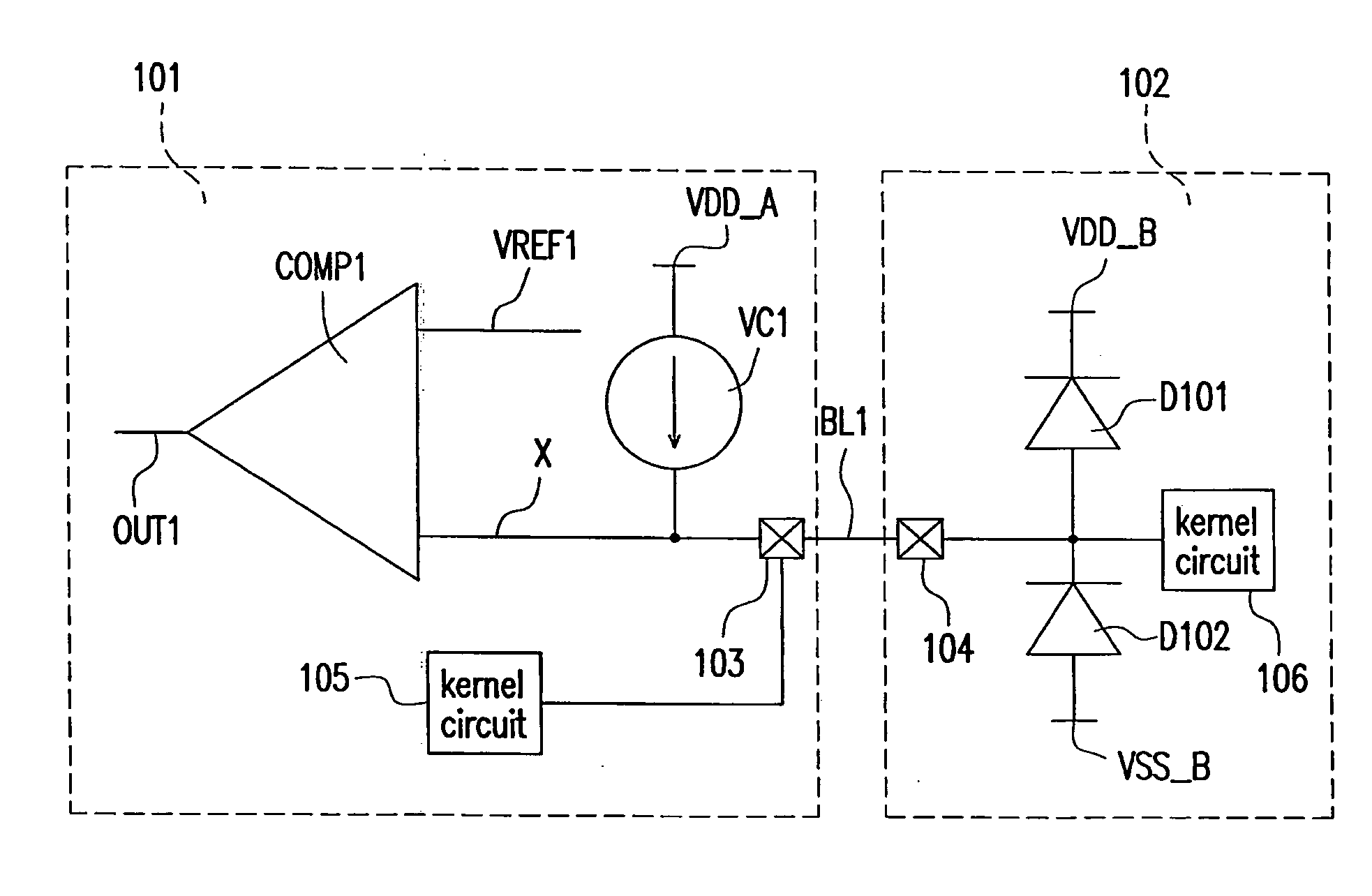
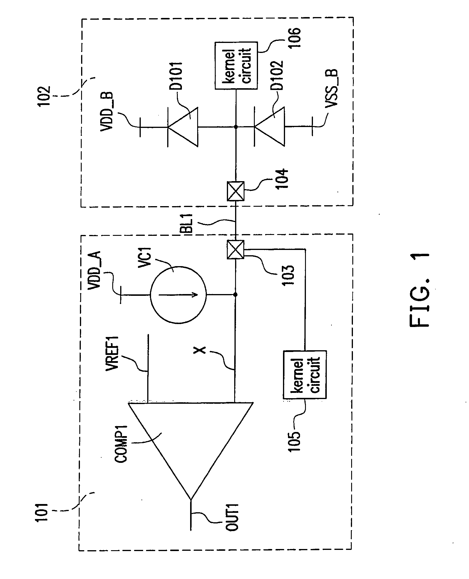
[0019]FIG. 1 is an embodiment of a connection testing apparatus. Referring to FIG. 1, a kernel circuit 105 of a first substrate (for example, an integrated circuit chip 101) and a kernel circuit 106 of a second substrate (for example, another integrated circuit chip 102) are connected with each other through an output end (for example, a pad 103), a connection BL1, and another output end (for example, a pad 104). The connection BL1 may be a weld line between the pad 103 and the pad 104. The connection testing apparatus is used to test the connection BL1 between the chip 101 and the chip 102.

[0020]In this embodiment, the chip 101 finishes the test of the connection BL1 by using a built-in test circuit. The built-in test circuit includes a charge source VC1 and a comparator COMP1. The chip 102 includes a first charge draining unit D101 and a second charge draining unit D102. The charge draining unit D101 and the charge draining unit D102 are both coupled to the second end (i.e., the p...


PUM


Abstract

A connection testing apparatus, a connection testing method, and a chip using the same are provided. The method can be used for testing connections between chips, so as to solve the problems that a conventional multi-chip connection test needs a plenty of test patterns, resulting in a long test time and a high test cost, and the condition of a connection failure is hard to be analyzed after a test failure. In the present invention, a voltage variation caused when an ESD element in a chip is conducted and a comparison circuits are used to determine whether a connection is correct. Furthermore, the test apparatus is built in the chip, so that the connection test may be accomplished quickly and efficiently. Once a connection failure occurs, the failed connection pin can also be found, so as to be favorable for engineering analysis and thereby effectively saving the test cost.

Description

BACKGROUND OF THE INVENTION[0001]1. Field of the Invention[0002]The present invention relates to a connection testing apparatus and method, and more particularly to a method of testing whether connection points of chips in a multi-chip package are truly connected by using a voltage variation caused by a current path.[0003]2. Description of Related Art[0004]With the advancement of science and technology, consumer electronics products are in more and more demand. In these days when motility and action ability are paid more attention to, a conventional large-scale tool providing powerful functions is gradually abandoned by people and replaced with a highly portable mobile electronic product with perfect functions. Some new-era products emerge as the times require, such as portable videodisc systems and mini personal computers. However, due to the significant addition of functions, the number of external electronic elements is greatly increased, such as memories and power module element...

Claims


Application Information

Patent Timeline
IPC IPC(8): G01R31/02
CPCG01R31/2853G01R31/31905G01R31/318505G01R31/31717
Inventor CHENG, JU-TIENTSENG, YIH-LONGLEO, HON-YUANYEN, CHENG-CHI
Owner HIMAX DISPLAY INC
Why Eureka
Try Eureka