Method for manufacturing organic electroluminescent device

a manufacturing method and electroluminescent technology, applied in semiconductor devices, coatings, nanotechnology, etc., can solve the problems of production equipment and energy efficiency, low light emission efficiency, and low production yield in the manufacturing process, and achieve high light emission efficiency, long life and suitability, and low voltage driving

Active Publication Date: 2009-03-26
MERCK PATENT GMBH
View PDF6 Cites 15 Cited by
  • Summary
  • Abstract
  • Description
  • Claims
  • Application Information

AI Technical Summary

Benefits of technology

[0030]It was achieved by the invention to provide a method of manufacturing an organic electroluminescent device by

Problems solved by technology

Therefore, the light emission efficiency is very low.
On the other hand, the vapor deposition process which is usually applied in the production of the organic EL device using a low molecular weight compound causes problems of production equipment and energy efficiency when the organic EL element having enlarged area is manufactured, and it is thought that a printing method including a ink-jet printing method and a screen printing method or a coating method such as a spin coating method and a cast coating method are desirable.
Particularly, in the case of the phosphorescent light emission device, it is difficult to deposit plural phosphorescent dopants in the same ratio in every times of manufactur

Method used


Image

  • Method for manufacturing organic electroluminescent device
  • Method for manufacturing organic electroluminescent device
  • Method for manufacturing organic electroluminescent device

Examples


example 1

Preparation of Organic EL Device 1-1

(Constitution and Forming Method of Each of Constituting Layers)

[0335]1) Cathode: Al (Vapor deposition)

[0336]2) Cathode buffer layer: LiF (Vapor deposition)

[0337]3) Electron transfer layer: Alq3 (Tg: 175° C.), Dispersion liquid coating, Dissolvable range of solubility parameter: 8.8 to 10.0

[0338]4) Positive hole blocking layer: BAlq (Tg: 100° C.), Dispersion liquid coating, Dissolvable range of solubility parameter: 8.8 to 10.6

[0339]5) Light emission layer: PVK+PD-1 (Tg: >200° C.), Solution coating, Dissolvable range of solubility parameter: 8.6 to 10.0

[0340]6) Positive hole transfer layer: PEDOT / PSS (Tg: >200° C., Dispersion liquid coating, Dissolvable range of solubility parameter: >14.8

[0341]7) Anode: ITO (Vapor deposition)

[0342]8) Glass substrate

[0343](Preparation of Organic EL Device)

[0344]An anode was formed by patterning on a substrate, NA-45 manufactured by NH Technoglass Co., Ltd., having a size of 100 mm×100 mm×1.1 mm, on which an ITO (i...

example 2

Preparation of Organic EL Device 2-1

(Constitution and Forming Method of Each of Constituting Layers)

[0449]1) Cathode: Al (Vapor deposition)

[0450]2) Cathode buffer layer: LiF (Vapor deposition)

[0451]3) Positive hole blocking layer: BAlq (Tg: 100° C.), Dispersion liquid coating, Dissolvable range of solubility parameter: 8.8 to 10.6

[0452]4) Light emission layer: OC-12 (Tg: 120° C.)+DP-1, Dispersion liquid coating, Dissolvable range of solubility parameter: 8.6 to 10.0

[0453]5) Second positive hole transfer layer: OC-4 (Tg: 140° C.), Dispersion liquid coating, Dissolvable range of solubility parameter: 8.6 to 10.6

[0454]6) First positive hole transfer layer: PEDOT / PSS, Dispersion liquid coating, Dissolvable range of solubility parameter: >14.8

[0455]7) Anode: ITO (Vapor deposition)

[0456]8) Glass substrate

(Preparation of Organic EL Device)

[0457]An anode was formed by patterning on a substrate, NA-45 manufactured by NH Technoglass Co., Ltd., having a size of 100 mm×100 mm×1.1 mm, on which a...

example 3

Preparation of Full Color Displaying Apparatus

(Blue Light Emission Organic EL Device)

[0502]Blue Light Emission Organic Device 2-1B was prepared in the same manner as in Organic EL Device 2-1 in Example 2 except that PD-1 was replaced by PD-9.

(Green Light Emission Organic EL Device)

[0503]Organic EL Device 2-1 prepared in Example 2 was used as a green light emission organic EL device.

(Red Light Emission Organic EL Device)

[0504]Red Light Emission Organic Device 2-1R was prepared in the same manner as in Organic EL Device 2-1 in Example 2 except that PD-1 was replaced by PD-6.

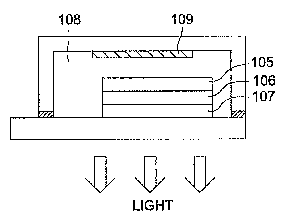
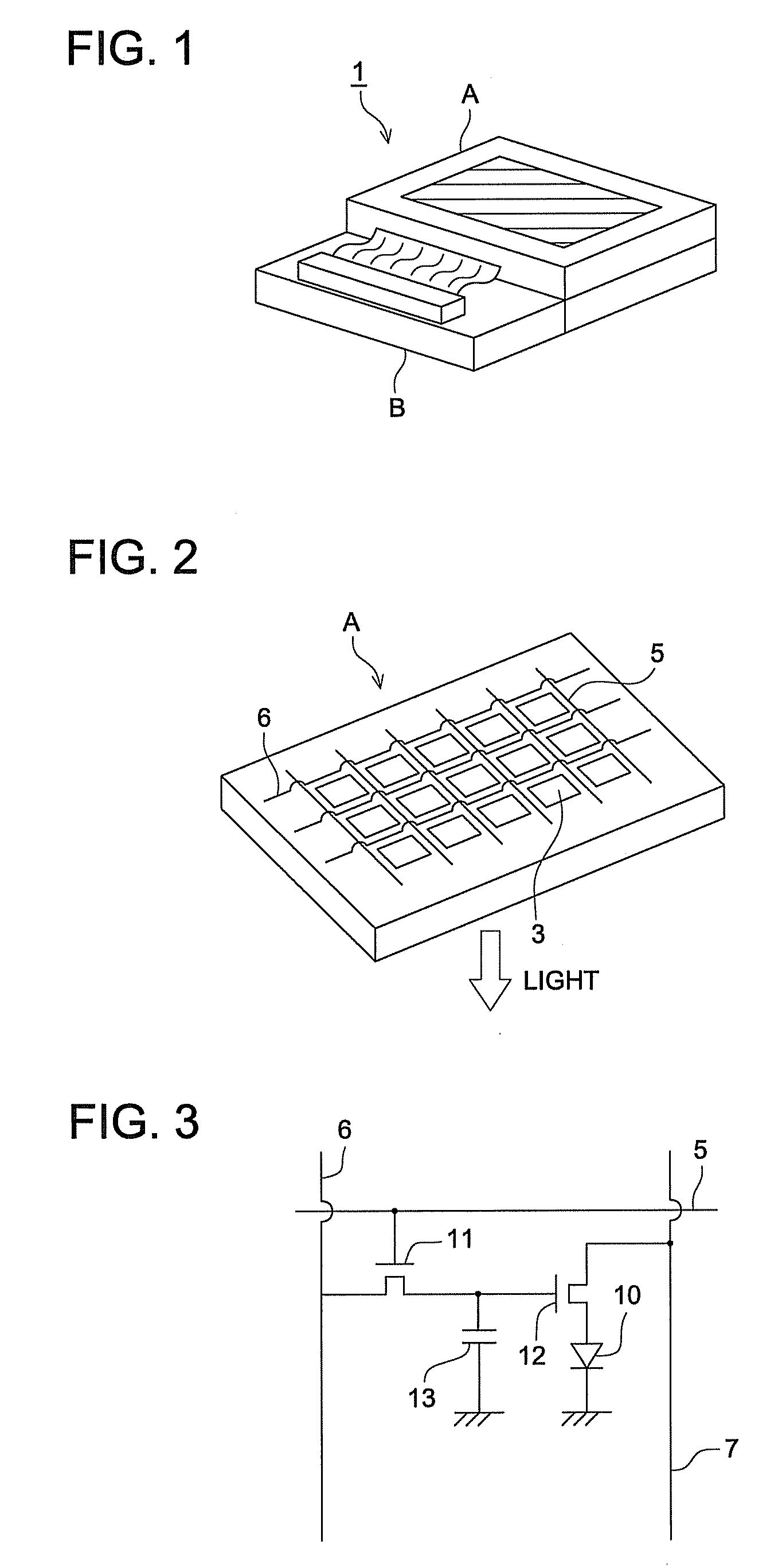
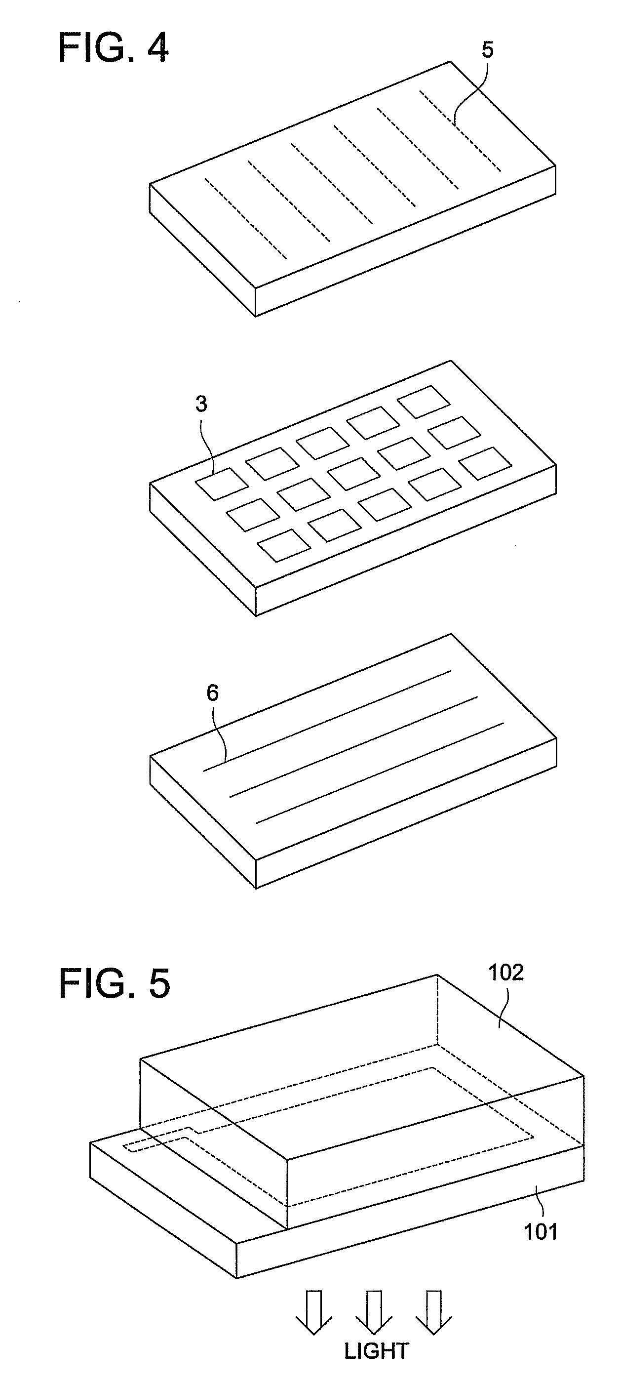
[0505]An active matrix type full color displaying apparatus having the shape displayed in FIG. 1 was prepared by arranging the organic EL devices of blue, green and red on the same substrate. A schematic drawing of the displaying portion A of thus prepared displaying apparatus is only displayed in FIG. 2. The displaying portion had a wiring including plural scanning lines 5 and data lines 6 and plural pixels 3 incl...


PUM


Abstract

Disclosed is an organic EL device having high external quantum efficiency, long emission life and low driving voltage. Also disclosed are an illuminating device and a display. Specifically disclosed is an organic electroluminescent device comprising, on a supporting substrate, at least an anode, a cathode and an organic compound layer which is arranged between the anode and the cathode and includes at least one light-emitting layer. This electroluminescent device is characterized in that the anode, cathode and organic compound layer are respectively formed by coating.

Description

FIELD OF THE INVENTION[0001]This invention relates to a method for manufacturing an organic electroluminescent device.BACKGROUND OF THE ART[0002]Hitherto, electroluminescent display, hereinafter referred to as ELD, is known as a light emission type electronic displaying device. As the constitution element of the ELD, inorganic electroluminescent devices and organic electroluminescent devices, hereinafter also referred to as organic EL device, can be cited. The inorganic electroluminescent device which is applied as flat type light sources requires a high alternating-current voltage for driving as the light emitting device.[0003]Meanwhile, the organic EL device is composed of a cathode, an anode and a light emission layer containing a light emission substance placed between the cathode and the anode, and is a light emission device in which electrons and positive holes are injected into the light emission layer to form excitons by recombination thereof and light emitted by inactivatio...

Claims


Application Information

Patent Timeline
IPC IPC(8): B05D5/06
CPCB82Y20/00B82Y30/00H01L27/3211H01L51/0003H01L2251/5369H01L51/5016H01L51/5036H01L51/56H01L51/0007H10K59/35H10K71/15H10K71/12H10K50/125H10K50/11H10K2101/10H10K2102/331H10K71/00
Inventor TAKA, HIDEOKITA, HIROSHIANDO, HIROAKI
Owner MERCK PATENT GMBH
Why Eureka
Try Eureka