Trench mosfet and method of manufacture utilizing four masks

a mosfet and mask technology, applied in the field of manufacturing of mosfets, can solve the problems of further difficulty in reducing cell pitch and limited cell pitch of mosfets, and achieve the effects of reducing manufacturing cost, improving critical alignment variation, and improving cell pitch

Inactive Publication Date: 2009-04-02
INPOWER SEMICON
View PDF5 Cites 26 Cited by
  • Summary
  • Abstract
  • Description
  • Claims
  • Application Information

AI Technical Summary

Benefits of technology

[0007]In accordance with the principles of the invention trench MOSFET structures are provided and methods are provided for forming such a trench MOSFET structure having an improved cell pitch and reduced manufacturing cost. The methods utilize a combination of chemical mechanical planarization (“CMP”) and self-aligned spacer techniques. In a first embodiment of the invention, the number of masking layers is reduced to four, and critical alignment variation is significantly improved through self-alignment.

Problems solved by technology

However, reducing cell pitch of MOSFETs is limited by the particulars of the MOSFET cell structure and the specific process, such as the alignment and the contact etch, used to manufacture the MOSFET.
Reducing cell pitch is made further difficult by limitations of the manufacturing process technology such as the minimum critical dimensions that the photolithography tools are configured to resolve, the minimum required spacing between different cell regions as dictated by the design rules, and the misalignment tolerances.

Method used


Image

  • Trench mosfet and method of manufacture utilizing four masks
  • Trench mosfet and method of manufacture utilizing four masks
  • Trench mosfet and method of manufacture utilizing four masks

Examples


first embodiment

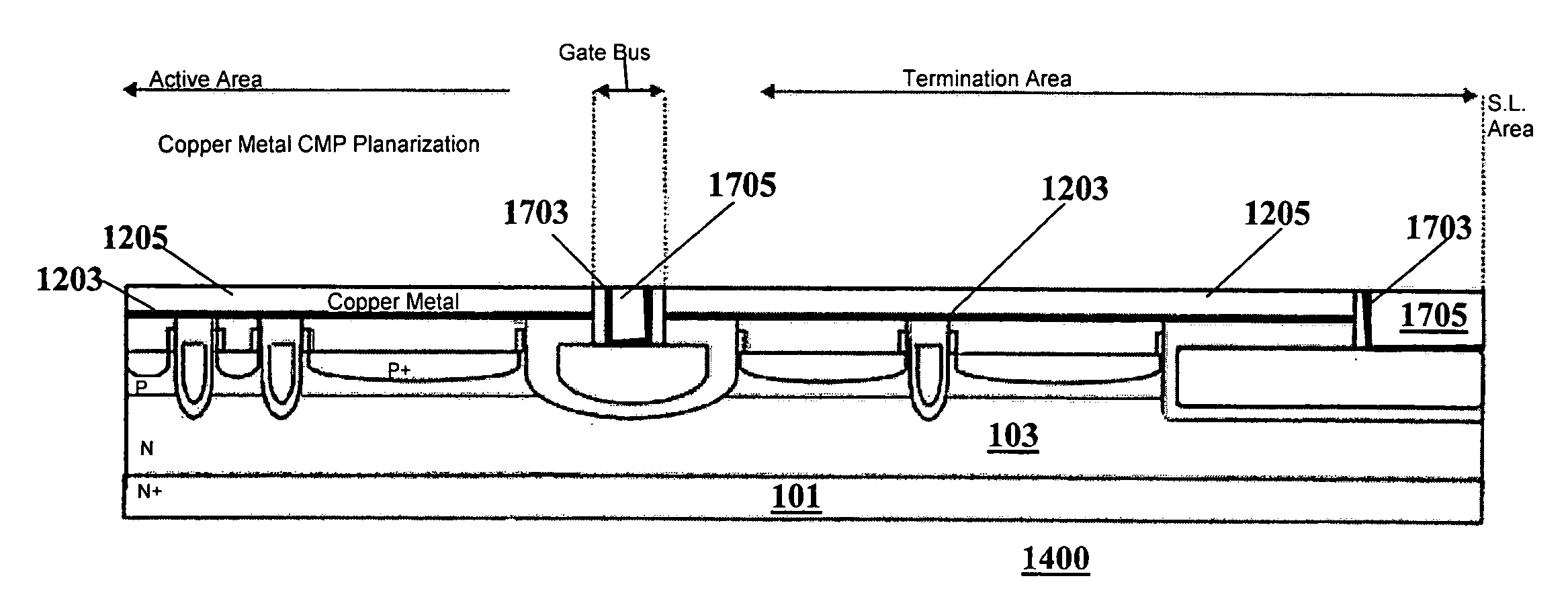
[0018]A first trench MOSFET is manufactured utilizing four mask layers, tungsten plug contact fillings and CMP planarization to shrink the cell pitch and reduce manufacturing cost The first embodiment as shown in FIGS. 1 through 7, inclusive, illustrates the manufacture of a trench DMOS (Double—Diffused MOSFET) device 100 and a termination structure.

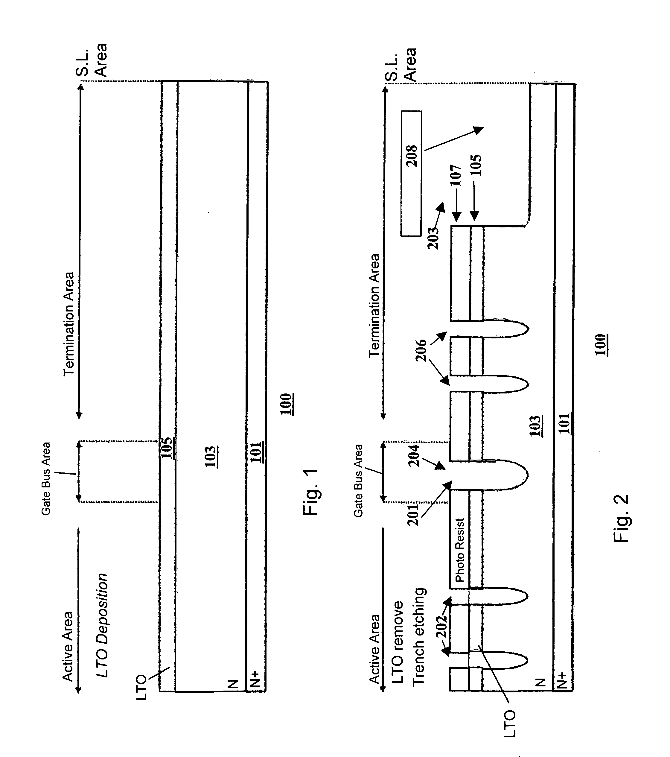
[0019]Turning now to FIG. 1, an N type epitaxial layer 103 is formed on a heavily doped N+ substrate 101. A thick SiO2 low temperature oxide (LTO) film 105 is formed by thermal oxidation.

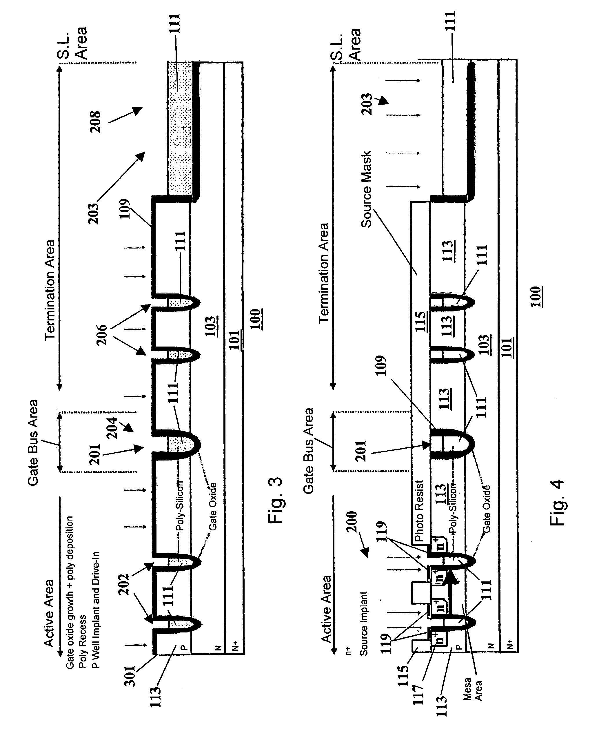
[0020]A trench mask 107, the first of the four masks, is deposited on LTO film 105 to define openings of the trench gate 201 and termination 203. Active region 200, trenches 202, gate bus trench 204, and termination trench 208 are then etched through the SiO2 film 105 and into the Si substrate to a depth range of 0.8 to 1.8 um. FIG. 2 shows the structure after trench mask definition.

[0021]After a sacrificial oxidation and an oxide removal, a gate oxide l...

second embodiment

[0049]In the invention shown in FIGS. 8 through 13, inclusive, a new three mask layer process using a self-aligned contact is provided to form a trench MOSFET device 800. The three mask layer process helps to reduce the mesa dimension and to remove the critical alignments thereby increasing cell density and lowering on-resistance.

[0050]As in the first embodiment an N type epitaxial layer 103 is formed on a heavily doped N+ substrate 101. P-body and source area formations, 801, 803, respectively, are created by Boron and Arsenic or Phosphorus ion implantation without any masks through whole wafer. A proper thermal annealing is performed after implantations.

[0051]A first mask, a trench mask is utilized to define the opening of the trench gate 201 and termination 203.

[0052]After a sacrificial oxidation and an oxide removal, a gate oxide layer 809 is thermally grown followed by thick Poly-Silicon refill layer 811. A mask is not used, nor is a mask needed, to define the gate bus area 201...


PUM


Abstract

In accordance with the invention, a trench MOSFET semiconductor device is manufactured in accordance with a process comprising the steps of: providing a heavily doped N+ silicon substrate; utilizing a first mask to define openings for the trench gate and termination; utilizing a second mask as a source mask with openings determining the size and shape of a diffused source junction depth; utilizing a third mask as a contact mask to define contact hole openings; and utilizing a fourth mask as a metal mask, whereby only the first, second, third and fourth masks are utilized in the manufacture of the trench MOSFET semiconductor device.

Description

FIELD OF THE INVENTION[0001]This invention pertains to the manufacture of semiconductor devices, in general, and to the manufacture of semiconductor devices comprising trench power MOSFET (metal-oxide-semiconductor field effect transistor) devices, in particular.[0002]Trench power MOSFET devices are used in many applications including power supplies, battery chargers, computers, and cell phones. The prior process to manufacture these devices typically utilizes six to eight masking layers. Because of the large quantity of wafers now manufactured, and the cost sensitive nature of the power MOS business, it is very desirable to simplify the process by reducing the number of masks.[0003]A trench MOSFET is a transistor in which the channel is formed vertically and the gate is formed in a trench extending between the source and drain. The trench, which is lined with a thin insulator layer such as an oxide layer and filled with a conductor such as poly-silicon, allows less constricted curr...

Claims


Application Information

Patent Timeline
Patent Type & Authority Applications(United States)
IPC IPC(8): H01L29/00H01L21/425
CPCH01L29/0661H01L29/407H01L29/4236H01L29/456H01L29/7813H01L29/66727H01L29/66734H01L29/7811H01L29/66719
Inventor SU, SHIH TZUNGZENG, JUNSUN, POITU, KAO WAYCHEN, TAI CHIANGLV, LONGWANG, XIN
Owner INPOWER SEMICON
Why Eureka
Try Eureka