Liner for tungsten/silicon dioxide interface in memory

a technology of tungsten and silicon dioxide, applied in the direction of diodes, semiconductor devices, electrical apparatus, etc., can solve the problems of reduced ability to maintain the electrical component on the semiconductor wafer, weakened electrical components, and higher failure rate, so as to optimize the formation of junction diodes and enhance adhesion

Active Publication Date: 2009-04-02
SANDISK TECH LLC
View PDF9 Cites 1 Cited by
  • Summary
  • Abstract
  • Description
  • Claims
  • Application Information

AI Technical Summary

Benefits of technology

[0005]A semiconductor wafer assembly includes a base of dielectric. A layer of silicon is deposited thereover. A metal hard mask is deposited over the silicon. A dielectric hard mask is deposited over the metal hard mask. Photoresist is deposited over the dielectric hard mask, whereby a plurality of sacrificial columns is formed from the layer of metal hard mask through the photoresist such that the sacrificial columns extend out from the silicon layer. An interface layer is disposed between the layer of conductive material and the layer of hard mask to enhance adhesion between each of the plurality of sacrificial columns and the layer of conductive material to optimize the formation of junction diodes out of the silicon by preventing the plurality of sacrificial columns from being detached from the layer of silicon prematurely.

Problems solved by technology

As the electrical component gets smaller to accommodate the compression requirements, the electrical component is weakened.
Hence, the ability to maintain the electrical component on the semiconductor wafer is reduced, resulting in a higher rate of failure.

Method used


Image

  • Liner for tungsten/silicon dioxide interface in memory
  • Liner for tungsten/silicon dioxide interface in memory
  • Liner for tungsten/silicon dioxide interface in memory

Examples


example 1

[0029]The thickness of the interface layer 62 may be in a range between five and ten nanometers, inclusive. The range of widths of the pillars after the clean portion of the fabrication process may be between 53 nm and 69 nm when the interface layer 62 is fabricated from titanium nitride. With respect to this example of the invention, the titanium nitride interface layer 62 may have a ratio of titanium and nitrogen as approximately 1:1. None of the junction diodes 22 fell from the hard mask layer 54 and peeling did not occur.

example 2

[0030]The thickness of the interface layer 62 may be in a range between five and ten nanometers, inclusive. The range of the widths of the pillars after the clean portion of the fabrication process may be between 72 nm and 80 nm when the interface layer 62 is fabricated from tungsten nitride. In this example, a nitrogen flow of 43% was present. None of the junction diodes 22 fell from the hard mask layer 54 and peeling did not occur.

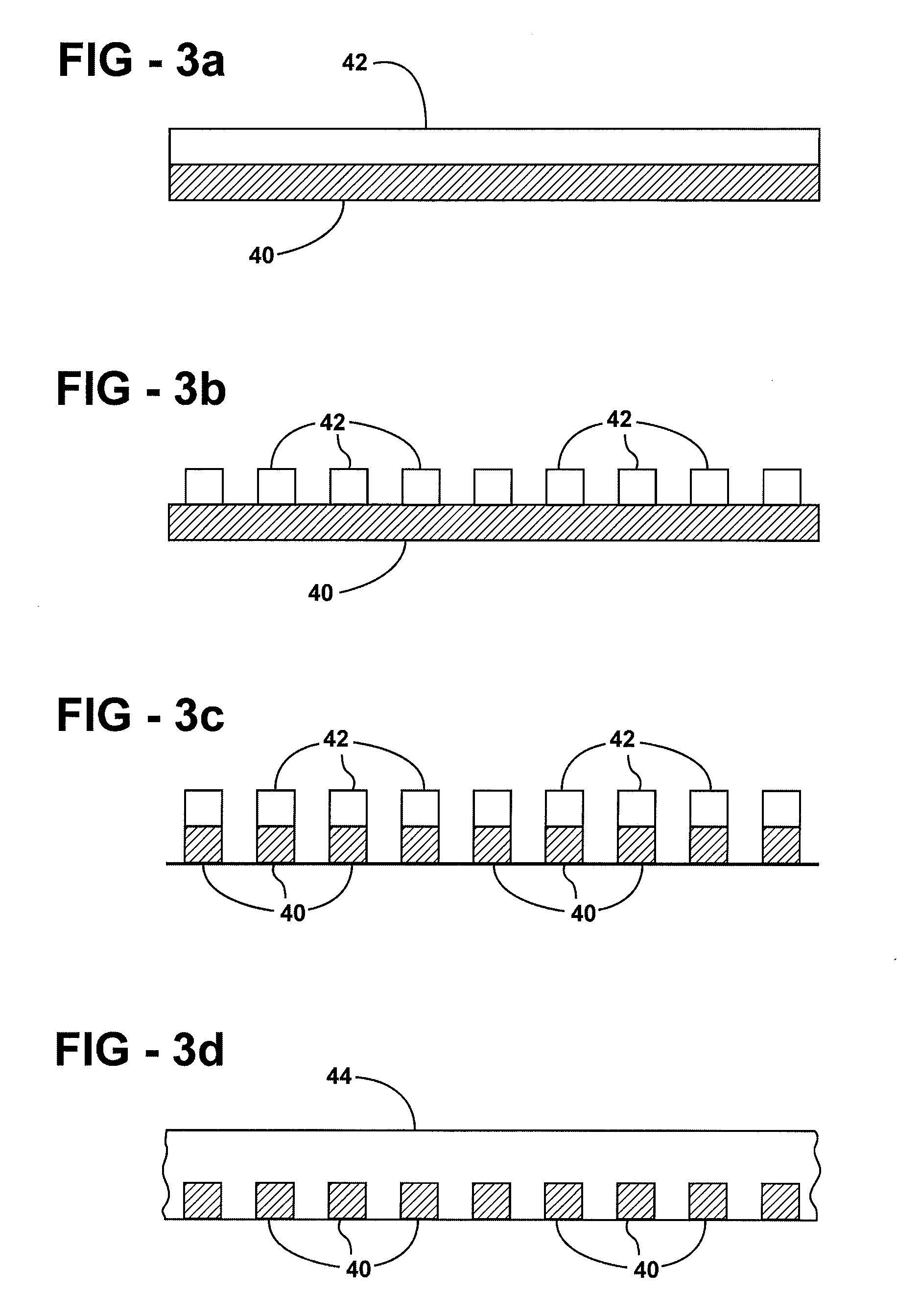
[0031]Referring to FIG. 5d, the metal hard mask 58 is etched. The metal hard mask 58 may be etched in a separate step from the other layers due to the differences in the chemistry needed when etching the metal hard mask 58.

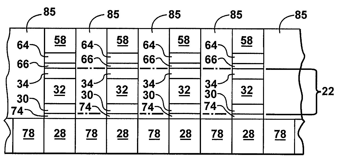
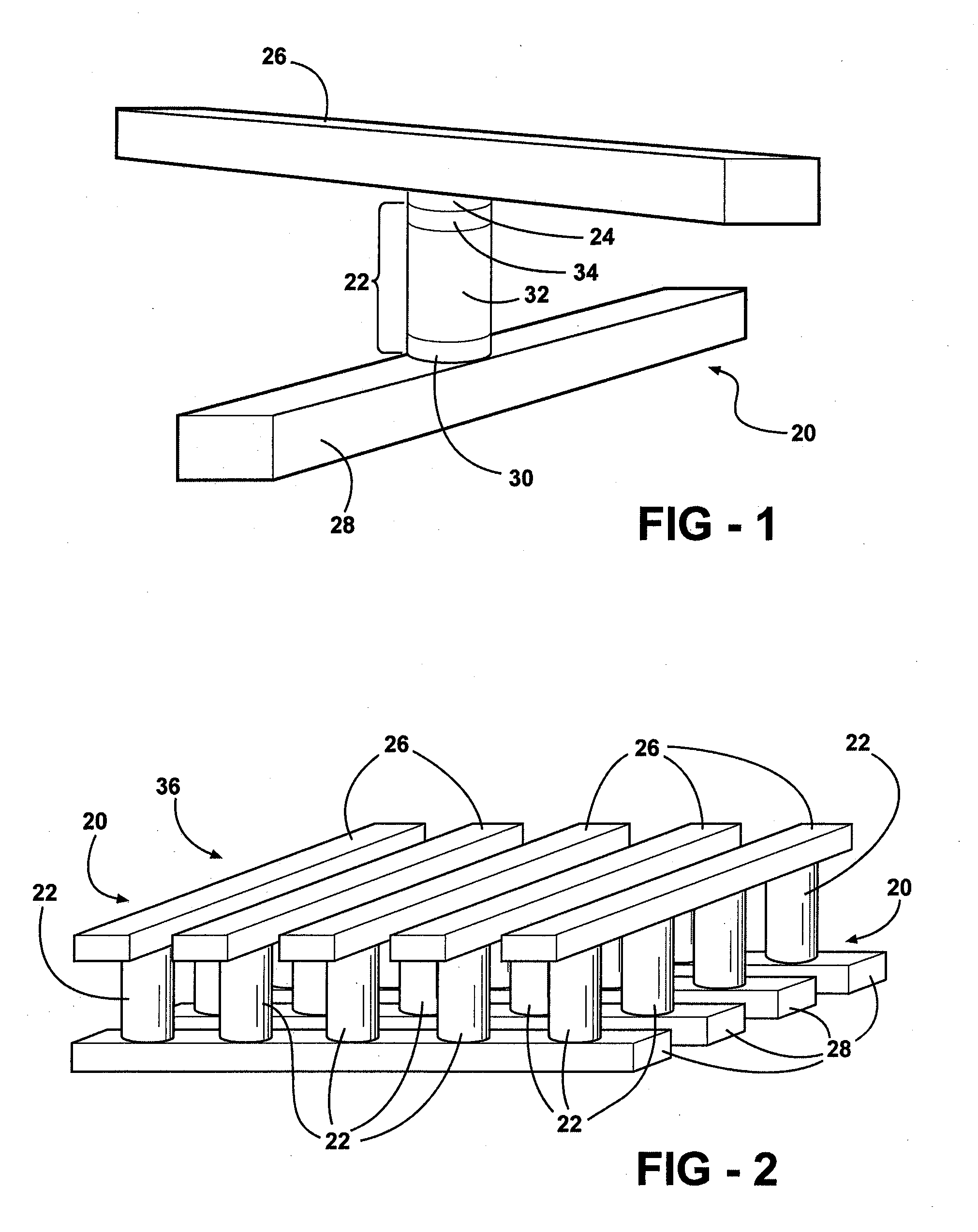
[0032]After the metal hard mask 58 has been etched, the junction diodes 22 are formed, as is shown in FIG. 5e. A single etch step forms the dielectric rupture antifuses 24, as well as converts all three layers of silicon 68, 70, 72 into the junction diodes 22 having the heavily doped semiconductor layer 30, the intermediate layer 32 an...


PUM

PropertyMeasurementUnit
thicknessaaaaaaaaaa
diameteraaaaaaaaaa
diameteraaaaaaaaaa

Abstract

A semiconductor wafer assembly includes a base of dielectric. A layer of silicon is deposited thereover. A metal hard mask is deposited over the silicon. A dielectric hard mask is deposited over the metal hard mask. Photoresist is deposited over the dielectric hard mask, whereby a plurality of sacrificial columns is formed from the layer of metal hard mask through the photoresist such that the sacrificial columns extend out from the silicon layer. An interface layer is disposed between the layer of conductive material and the layer of hard mask to enhance adhesion between each of the plurality of sacrificial columns and the layer of conductive material to optimize the formation of junction diodes out of the silicon by preventing the plurality of sacrificial columns from being detached from the layer of silicon prematurely due to the sacrificial columns peeling or falling off.

Description

BACKGROUND ART[0001]The invention generally relates to a structure used to enhance the integrity of devices formed on a semiconductor wafer. More particularly, the invention relates to a structure used to enhance the integrity of devices formed generally perpendicular to a semiconductor wafer.[0002]Devices made from semiconductor materials are used to create memory circuits in electrical components and systems. Memory circuits are the backbone of such devices as data and instruction sets are stored therein. Minimizing the amount of natural resources and space consumed by memory circuits is a primary motivation in the designing of such circuits. As the design of memory circuits has moved from two-dimensional designs to three-dimensional designs, more emphasis is being made to minimize the space required to build structures, while maintain the integrity and strength of same, which becomes more important as more elements are incorporated into a space, the greater the cost in having to ...

Claims


Application Information

Patent Timeline
Patent Type & Authority Applications(United States)
IPC IPC(8): H01L29/788H01L21/4763
CPCH01L27/1021H01L27/101
Inventor TANAKA, YOICHIRORADIGAN, STEVEN J.RAGHURAM, USHA
Owner SANDISK TECH LLC
Why Eureka
Try Eureka