Method for making a conductive film and a probe card using the same

a technology of conductive film and probe card, which is applied in the manufacture of cables/conductors, instruments, measurement devices, etc., can solve the problems of only good vertical type probe cards, bottlenecks in the design of vertical type probe cards with pitch, and increasing the difficulty of on-wafer testing tasks, etc., to achieve easy maintenance and large detection area

Inactive Publication Date: 2009-04-09
IND TECH RES INST
View PDF5 Cites 26 Cited by
  • Summary
  • Abstract
  • Description
  • Claims
  • Application Information

AI Technical Summary

Benefits of technology

[0008]The object of the present invention is to provide a method for manufacturing a conductive film and a probe card using the same, that can produce a low-cost, ease-to-maintain probe card with large area detection ability that is adapted for wafers of various bonding pad arrangements.

Problems solved by technology

However, as semiconductor manufacturers continue to shrink die geometries, which makes the task of on-wafer testing increasingly more difficult since pitches between bonding pads are becoming minute.
However, although such vertical type probe card is adapted for testing wafers 300 with a plurality of bonding pads arranged as arrays and is classified as high-end probe card with high pin count, it is bottlenecked for designing such vertical type probe card with pitch as small as 100 μm.
Therefore, such vertical type probe cards are only good for testing flip chip packaged IC.
Thus, their manufacturing cost is closely related to their pin counts, i.e. the higher the pin count is, the higher the manufacturing cost will be.
However, it is disadvantageous in that its manufacturing process is complex and it is bottlenecked for designing such MEMS type probe card with pitch smaller than 70 μm, thereby, such MEMS type probe can be very expensive.
In addition, it is limited to be used for testing wafers with bonding pad arrangement similar to that shown in FIG. 1.
In addition, the pin pitches of those currently available probe cards are limited by their manufacturing processes, which might not be able to meet the challenge of ultra fine pitch up to those smaller than 70 μm, high pin counts and full wafer testing.
However, such studies still limited in the aforesaid “one pin corresponding to one pad” manner, and thus suffer the same shortcomings.

Method used


Image

  • Method for making a conductive film and a probe card using the same
  • Method for making a conductive film and a probe card using the same
  • Method for making a conductive film and a probe card using the same

Examples


Embodiment Construction

[0032]For your esteemed members of reviewing committee to further understand and recognize the fulfilled functions and structural characteristics of the invention, several exemplary embodiments cooperating with detailed description are presented as the follows.

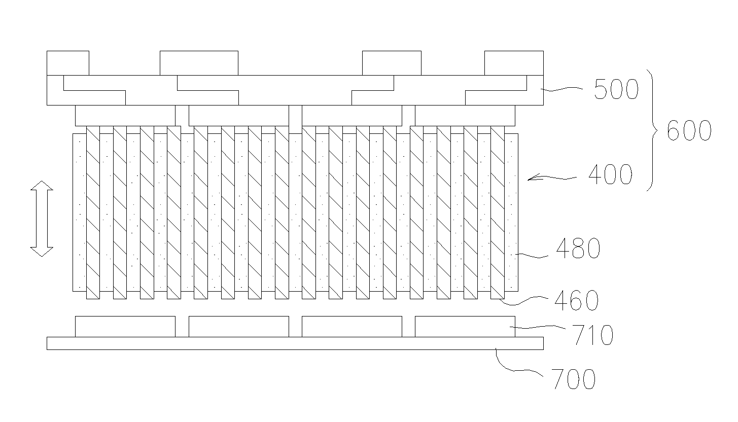
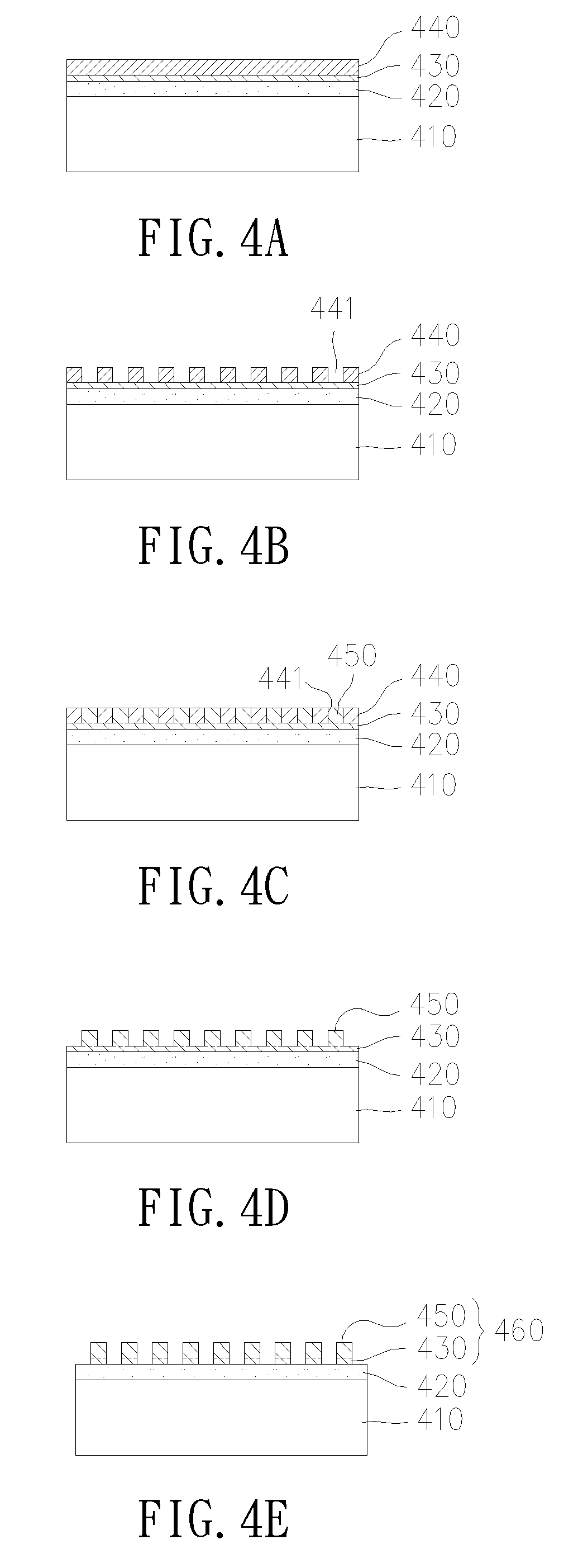
[0033]Please refer to FIG. 4A to FIG. 4H, which show sequentially the manufacturing of a conductive film, each representing a step in the manufacturing process. The manufacturing of the conductive film makes use of many micro / nano-technologies, such as micro / nano-scaled polymer film formation, LIGA process, and micro electroforming technology and the like.

[0034]In FIG. 4A, a silicon substrate 410 is provided, on which a micro scaled polymer film, made of a material such as PDMS or PI, is first being coated and used as a first insulating layer 420; and then on the first insulating layer 420, a nano-scaled metal layer, made of a metal such as nickel or copper, is formed by sputtering or electroless plating and used as a first me...


PUM

PropertyMeasurementUnit
diameteraaaaaaaaaa
aspect ratioaaaaaaaaaa
sizeaaaaaaaaaa

Abstract

A method for manufacturing a conductive film as well as the structure thereof and a probe card using the same are provided in the invention. The conductive film is substantially a stacked structure of a specific thickness formed by the adhering and stacking of at least an substrate in a vacuum environment by the use of surface processing and mechanical healing whereas each substrate has an array of metal micro-threads formed thereon, in which the plural metal micro-threads, each being wrapped in an insulating film, are arranged on the substrate to form the array in a unidirectional and single-layered manner by the use of a LIGA process and polymer thin film technology. In an exemplary embodiment, the insulating film can be a polymer thin film of high dielectric constant, being made of a material such as polydimethylsiloxane (PDMA) or polyimide (PI); and the metal micro-thread is made of a high conductivity and high strength Ni—Co alloy. Moreover, the so-formed conductive film can be cut into any desired dimensions by the use of an energy beam, such as laser beam, ion beam and plasma beam, etc. while combining the conductive film with a panel so as to be used for forming a probe card with large area detection ability that is low-cost, ease-to-maintain and capable of being adapted for wafers of various bonding pad arrangements.

Description

FIELD OF THE INVENTION[0001]The present invention relates to a method for manufacturing a conductive film and a probe card using the same, and more particularly, to a probe card capable of engaging more than one pin to a bonding pad that is adapted for wafer of various bonding pad arrangement.BACKGROUND OF THE INVENTION[0002]A probe card is an interface between an electronic test system and a semiconductor wafer. Its purpose is to provide an electrical path between the test system and the circuits on the wafer, thereby permitting the testing and validation of the circuits at the wafer level, usually before they are diced and packaged. That is, before hundreds of IC chips fixed on a wafer are diced into chips with a few square millimeters, “Wafer Test” should be performed utilizing such probe card to check quality of IC chips and thus screen out defectives. However, as semiconductor manufacturers continue to shrink die geometries, which makes the task of on-wafer testing increasingly...

Claims


Application Information

Patent Timeline
Patent Type & Authority Applications(United States)
IPC IPC(8): G01R1/067H01B13/00
CPCG01R1/07314Y10T29/49222G01R3/00G01R1/07378
Inventor WU, TUNG-CHUANCHOU, MIN-CHIEHLIN, HUNG-YI
Owner IND TECH RES INST
Why Eureka
Try Eureka