Method Of Generating X-Ray Diffraction Data For Integral Detection Of Twin Defects In Super-Hetero-Epitaxial Materials

a technology of super-hetero-epitaxial materials and x-ray diffraction data, which is applied in the direction of material analysis using radiation diffraction, instruments, measurement devices, etc., can solve the problems of difficult to achieve high-quality (i.e., defect-free) sige layers on silicon substrates, and thick growth of thick layers

Active Publication Date: 2009-04-23
NASA
View PDF2 Cites 21 Cited by
  • Summary
  • Abstract
  • Description
  • Claims
  • Application Information

AI Technical Summary

Benefits of technology

[0013]Another object of the present invention is to provide a nondestructive method of generating data indicative of twin defects present in rhombohedrally-grown, strained or lattice-matched cubic semiconductor alloys on the c-plane of trigonal crystal, and other super-hetero-epitaxial materials, where the data can be used for quality control in the production of semiconductor wafers.

Problems solved by technology

However, the growth of thick (i.e., greater than tens of nanometers), high-quality (i.e., defect free) SiGe layers on a silicon substrate is difficult to achieve because SiGe has a larger lattice constant than silicon.
This means that the SiGe layers close to the silicon substrate are strained, and severe defects (e.g., threading dislocations, twin defects such as bulk twin domain and micro-twin defects, cracks, delaminations, etc.) develop in the layers of SiGe that exceed a critical thickness of hundreds of nanometers, because of the lattice mismatch.
While such methods can yield high-quality, either strained or lattice-matched semiconductor alloys based on a wide variety of selected materials and substrates, problems can develop during fabrication that can affect the quality of the fabricated material.
For example, twin defects can be formed in such materials by one or both of (i) double position defects due to crystal structure differences between the epilayer and substrate, and (ii) stacking faults during epilayer growth.
However, TEM results in destruction of the material and is, therefore, only suitable for microscopic laboratory analysis or as a periodic or random sampling check on semiconductor materials being mass-produced.
This method is therefore not suitable for generating data for quality control during the fabrication of semiconductor wafers.

Method used


Image

  • Method Of Generating X-Ray Diffraction Data For Integral Detection Of Twin Defects In Super-Hetero-Epitaxial Materials
  • Method Of Generating X-Ray Diffraction Data For Integral Detection Of Twin Defects In Super-Hetero-Epitaxial Materials
  • Method Of Generating X-Ray Diffraction Data For Integral Detection Of Twin Defects In Super-Hetero-Epitaxial Materials

Examples


first embodiment

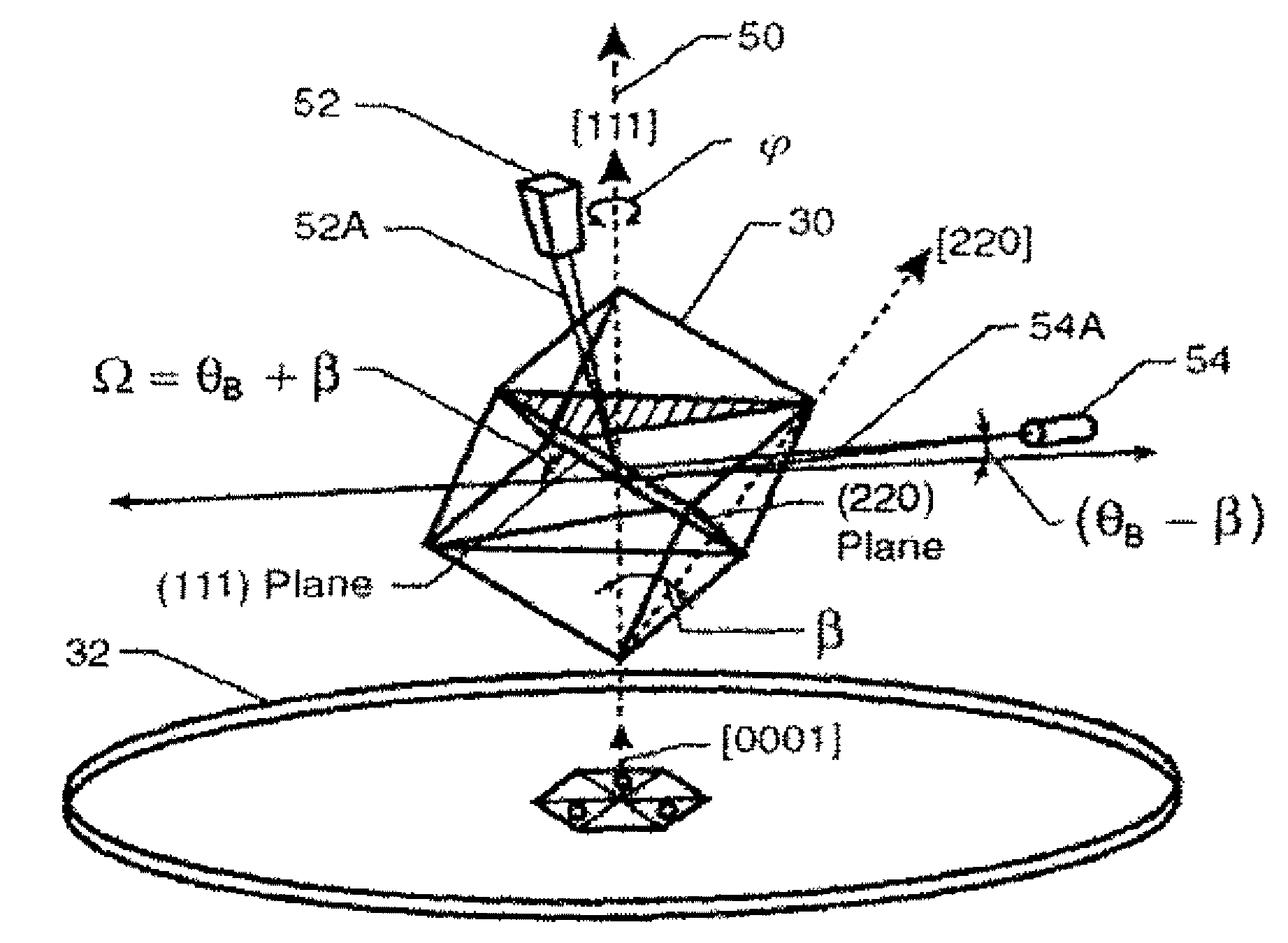
[0061]In the first embodiment, illustrated in FIG. 6, the following setup criteria apply:[0062](i) The goniometer angle Ω associated with X-ray beam 52A is set equal to the Bragg angle θB.[0063](ii) Detector 54 is positioned so that its direction of focus 54A is equal to 2*θB (i.e., the conventional Bragg-Brentano setup is used where θ=θB).[0064](iii) The alloy sample is positioned (e.g., via movement of the XRD system's sample holder) such that the [111] vector of structure 30 (i.e., the [111] vector is normal to the {111} crystal plane) makes an angle of χ=β relative to reference orientation 50 of the XRD system and lying in the common plane defined by X-ray beam 52A and direction of focus 54A.

[0065]The angle β is the inter-planar angle between the alloy's {111} crystal plane and the selected non-perpendicular plane (i.e., the {220} crystal plane in the illustrated example). As is known in the art, the inter-planar angle ˜ between two crystal planes is defined as

cos(β)=(h1h2+k1k2+...

second embodiment

[0073]Second and third test-ready position setups will now be explained with reference to FIGS. 7 and 8. As mentioned above, the first step is to calculate the Bragg angle θB for the alloy that will once again be SiGe for purpose of illustration. In the present invention illustrated in FIG. 7, the following setup criteria apply:[0074](i) The goniometer angle Ω is set equal to (θB+β) where β is once again the inter-planar angle described above.[0075](ii) Detector 54 is positioned so that its direction of focus 54A is equal to (θB−β)[0076](iii) The sample is positioned such that the [111] vector is aligned with the XRD system's reference orientation 50. That is, the tilt angle χ equals zero.

[0077]With the above-described test-ready positioning of the alloy, the XRD system is then operated as previously described for the first embodiment.

third embodiment

[0078]In a third embodiment illustrated in FIG. 8, the Bragg angle θB is calculated and the following setup criteria apply:[0079](i) The goniometer angle Ω is set equal to (θB−β) where β is once again the inter-planar angle described above.[0080](ii) Detector 54 is positioned so that its direction of focus 54A is equal to (θB+β).[0081](iii) The sample is positioned such that the [111] vector is aligned with the XRD system's reference orientation 50. That is, the tilt angle χ equals zero.

[0082]With the above-described test ready positioning of the alloy, the XRD system is then operated as previously described for the first embodiment.

[0083]In each of the above-described embodiments, the phrase “phiscan” assumes an azimuthal rotation of the sample being tested. However, the present invention is not so limited. That is, sample rotation may not be required in test set-ups that utilize multiple detectors to record diffraction data at the appropriate angles of φ where these angles lie in ...


PUM

PropertyMeasurementUnit
azimuthal angleaaaaaaaaaa
tilt angleaaaaaaaaaa

Abstract

A method provides X-ray diffraction data suitable for integral detection of a twin defect in a strained or lattice-matched epitaxial material made from components having crystal structures having symmetry belonging to different space groups. The material is mounted in an X-ray diffraction (XRD) system. In one embodiment, the XRD system's goniometer angle Ω is set equal to (θB−β) where θB is a Bragg angle for a designated crystal plane of the alloy that is disposed at a non-perpendicular orientation with respect to the {111) crystal plane, and β is the angle between the designated crystal plane and a {111} crystal plane of one of the epitaxial components. The XRD system's detector angle is set equal to (θB+β). The material can be rotated through an angle of azimuthal rotation φ about the axis aligned with the material. Using the detector, the intensity of the X-ray diffraction is recorded at least at the angle at which the twin defect occurs.

Description

CROSS-REFERENCE TO RELATED APPLICATIONS[0001]This application claims the benefit of the respective filing dates of, and incorporates by reference the entire respective disclosures of, the following commonly assigned U.S. Provisional Patent Applications: Ser. No. 60 / 980,780 filed on Oct. 18, 2007, Ser. No. 60 / 980,881 filed on Oct. 18, 2007, Ser. No. 60 / 980,878 filed on Oct. 18, 2007, Ser. No. 60 / 980,880 filed on Oct. 18, 2007, Ser. No. 60 / 980,876 filed on Oct. 18, 2007, and Ser. No. 60 / 980,871 filed on Oct. 18, 2007, each of which contains an overlap of inventive entity with the present application. In addition, this application incorporates by reference the entire disclosures of the following commonly assigned nonprovisional U.S. patent applications being filed on the same date as the present application: Ser. No. ______, entitled “EPITAXIAL GROWTH OF CUBIC CRYSTALLINE SEMICONDUCTOR ALLOYS ON BASAL PLANE OF TRIGONAL OR HEXAGONAL CRYSTAL; Ser. No. ______, entitled “HYBRID BANDGAP ENG...

Claims


Application Information

Patent Timeline
Patent Type & Authority Applications(United States)
IPC IPC(8): G01N23/207
CPCG01N23/207
Inventor PARK, YEONJOONCHOI, SANG HYOUKKING, GLEN C.ELLIOTT, JAMES R.
Owner NASA
Why Eureka
Try Eureka